
Method of manufacturing a thin dielectric layer using a heat treatment and a semiconductor device formed using the method
a technology of heat treatment and semiconductor devices, which is applied in the direction of semiconductor devices, electrical devices, transistors, etc., can solve the problems of high programming voltage, increase manufacturing costs, and increase manufacturing costs, so as to reduce the size of the transistor and the resulting storage cell, the effect of increasing capacitance coupling
Patent Information
- Authority / Receiving Office
- US · United States
- Patent Type
- Patents(United States)
- Current Assignee / Owner
- Publication Date
- 2007-03-13
Smart Images
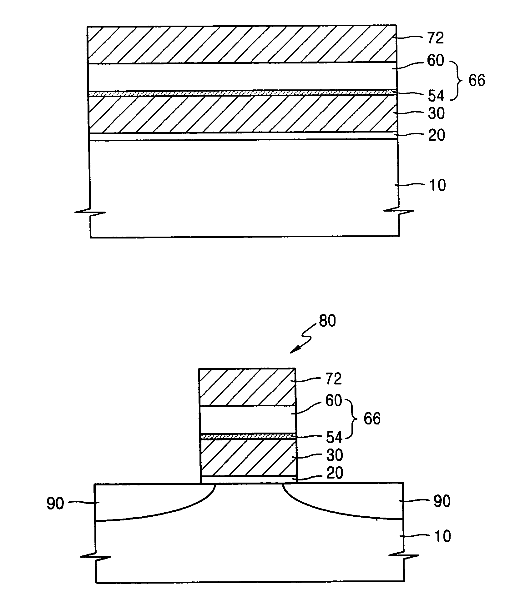
Figure 1 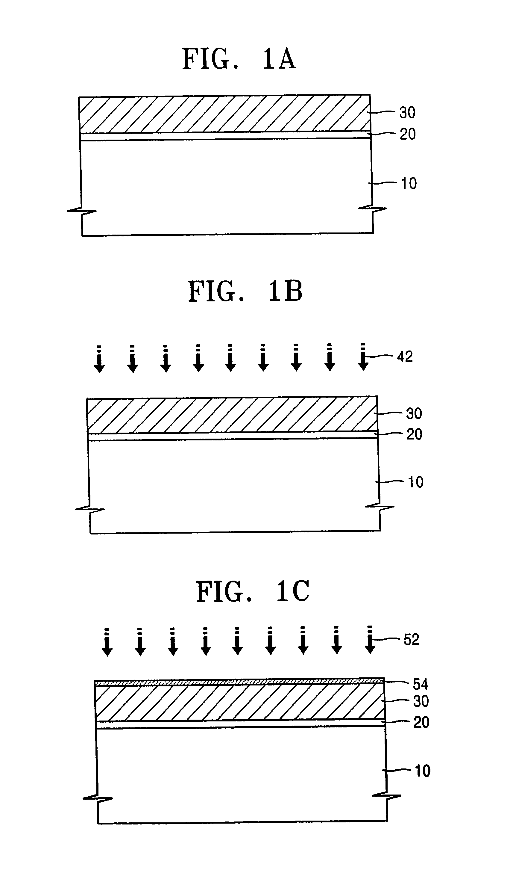
Figure 2 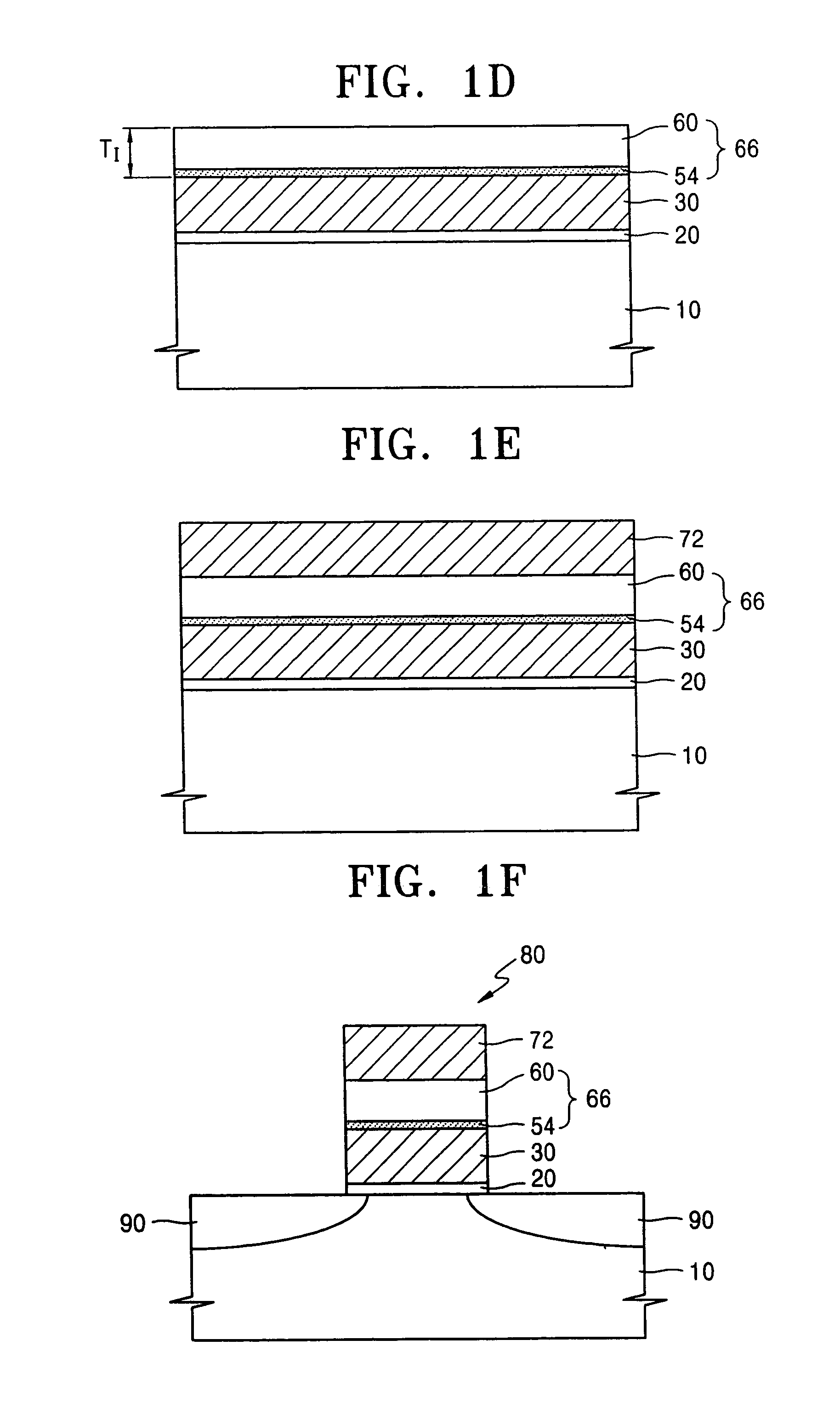
Figure 3
Abstract
Description
RELATED APPLICATIONS
[0001] This application is a divisional of U.S. application Ser. No. 10 / 832,952, filed on Apr. 27, 2004, now U.S. Pat. No. 7,041,557 which relies for priority upon Korean Patent Application Serial Number 2003-80574, filed Nov. 14, 2003, the contents of which are incorporated herein by reference, in their entirety.BACKGROUND OF THE INVENTION
[0002] Non-volatile memory devices find widespread application in electronic systems that do not receive continuous power, for example in applications where power is not always available, where power is frequently interrupted, and / or where low-power usage is desired. Example applications include mobile telecommunication systems, memory cards for storing music and / or image data, and system on a chip applications that include a processing unit and a memory unit.
[0003] Cell transistors in non-volatile memory devices commonly employ a stacked gate structure that is formed over a channel region of a substrate between source / drain regio...
Examples
Embodiment Construction
[0028]In the following description of preferred embodiments of the present invention and in the claims that follow, the term “on”, when referring to layers of material used in the fabrication of semiconductor devices, refers to a layer that is directly applied to an underlying layer, or refers to a layer that is above an underlying layer with an optional intermediate layer or layers therebetween. The thicknesses of the respective layers are not necessarily to scale in the drawings, but instead are exaggerated for clarity and to illustrate the various features of the present invention.
[0029]FIGS. 1A–1F are cross-sectional views of the fabrication of a semiconductor device in accordance with an embodiment of the present invention.
[0030]In FIG. 1A, a gate insulating layer 20 is formed to a thickness of 100 Å on a semiconductor substrate 10. In one embodiment, the semiconductor substrate comprises silicon material and the gate insulating layer comprises SiO2, or “oxide”.
[0031]A first co...