
High performance sub-micron P-channel transistor with germanium implant
Patent Information
- Authority / Receiving Office
- US · United States
- Current Assignee / Owner
- Publication Date
- 2001-05-01
- Estimated Expiration
- Not applicable · inactive patent
Smart Images
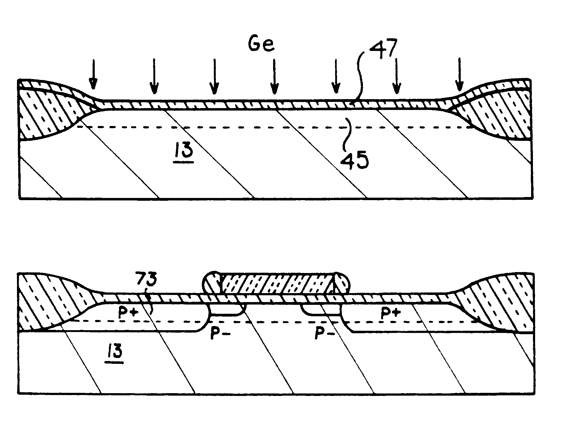
Figure 1 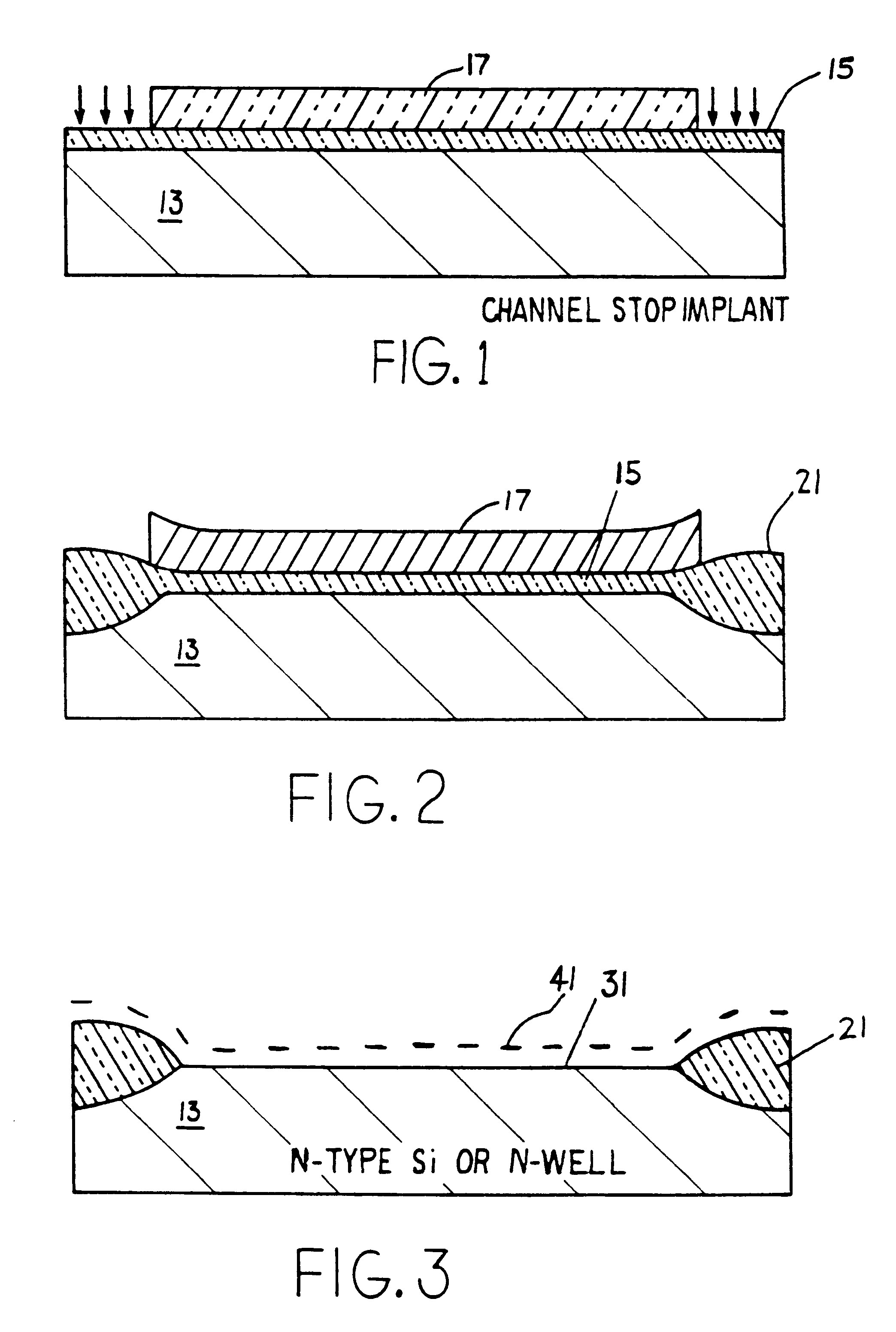
Figure 2 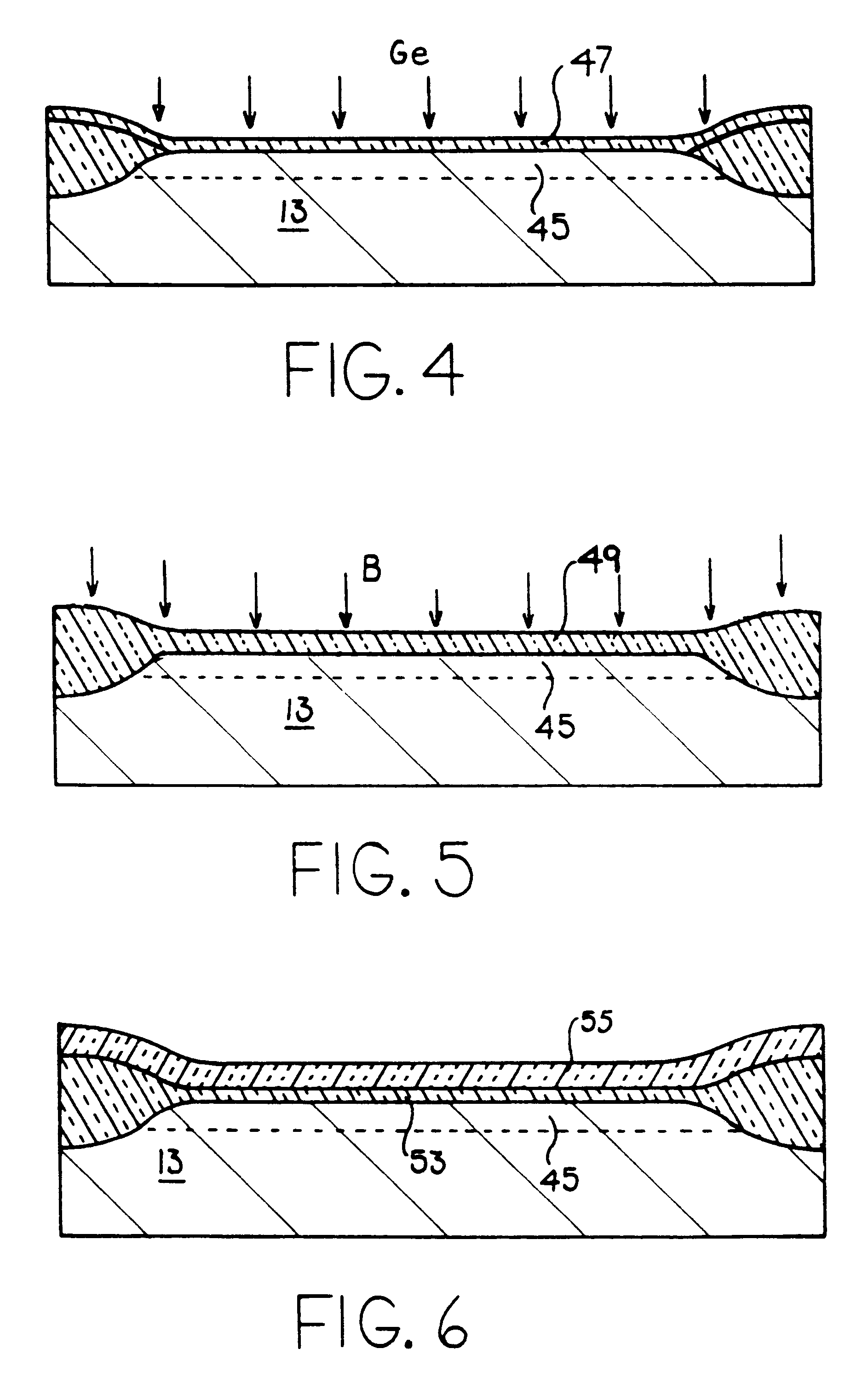
Figure 3
Abstract
Description
FIELD OF THE INVENTIONThis invention is related to semiconductor devices. Specifically it is related to high-performance sub-micron channel length P-channel MOS (metal-oxide-semiconductor) transistor (PMOS for short) for the Very Large Scale Integrated (VLSI) or the Ultra Large Scale Integrated (ULSI) circuits. It employs the use of Germanium implant into the channel regions of transistors to both pre-amorphize the channel surface to alleviate the channelling of subsequent enhancement implant required by threshold voltage Vt adjustment and to retard the diffusion of the boron dopants (from enhancement implant) in the region to form a very shallow enhancement implant profile.BACKGROUND OF THE INVENTIONThe invention uses various materials which are electrically either conductive, insulating or semiconducting, although the completed semiconductor circuit device itself is usually referred to as a "semiconductor". One of the materials used is silicon, which is used as either single cryst...
Examples
Embodiment Construction
FIG. 1 shows a cross-section of a semiconductor circuit during its fabrication. A silicon wafer 13 is prepared by forming a thin film of oxide 15 and then depositing nitride 17 over the thin oxide 15. The nitride is masked and etched in order to define active area (31, FIG. 3). The unmasked portions of the wafer 13 are then implanted with boron in order to increase parasitic field transistor threshold voltage V.sub.TF.
After the field implant, a thick layer of silicon oxide 21 is grown onto the wafer 13 to form field ox, as shown in FIG. 2. The growth of silicon oxide occurs in areas which are not covered by the nitride mask 17, but tends to encroach on the active area, marked AA. The encroachment is present around the edges of the nitride 17, as indicated by dashed lines 23, where the oxide 21 begins to "buck up" or lift the nitride 17.
The nitride 17 is then stripped and the wafer 13 is oxide etched in order to remove a top portion 41 of the field ox 21, as shown in FIG. 3. This red...