Check patentability & draft patents in minutes with Patsnap Eureka AI!

Method of forming isolation structure of semiconductor device

An isolation structure and semiconductor technology, applied in semiconductor/solid-state device manufacturing, solid fuel, special form of dry distillation, etc., can solve problems such as difficult to use, difficult to fill trenches in gaps between HDP oxide layers, and difficult to fill trenches

Inactive Publication Date: 2007-08-29
SK HYNIX INC
View PDF1 Cites 3 Cited by
  • Summary
  • Abstract
  • Description
  • Claims
  • Application Information

AI Technical Summary

Problems solved by technology

However, when the aspect ratio of the trench increases due to high integration, it becomes difficult to gap fill the trench with the HDP oxide layer
If the aspect ratio of the trench is higher than 4, it becomes difficult to gap fill the trench with current HDP equipment
In currently developed 60nm NAND flash devices, the aspect ratio of the isolation trenches is about 5.5, which makes it difficult to gap fill the trenches with the HDP oxide layer

Method used


Image

  • Method of forming isolation structure of semiconductor device
  • Method of forming isolation structure of semiconductor device

Examples


Embodiment Construction

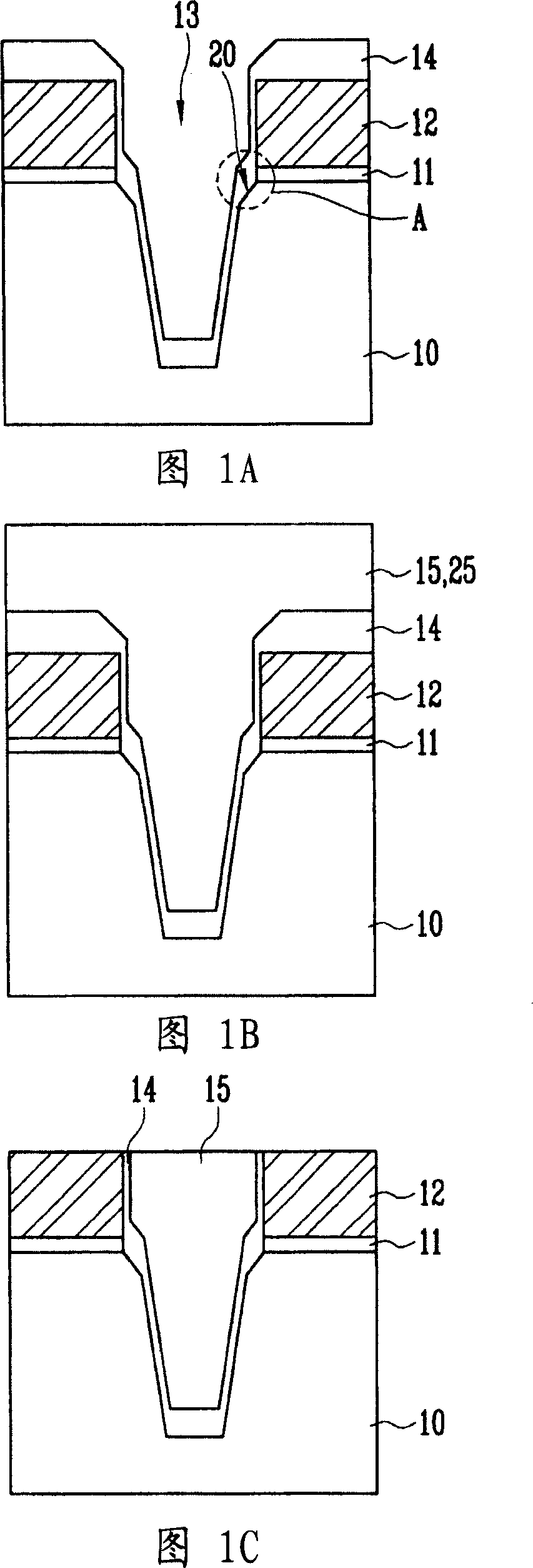
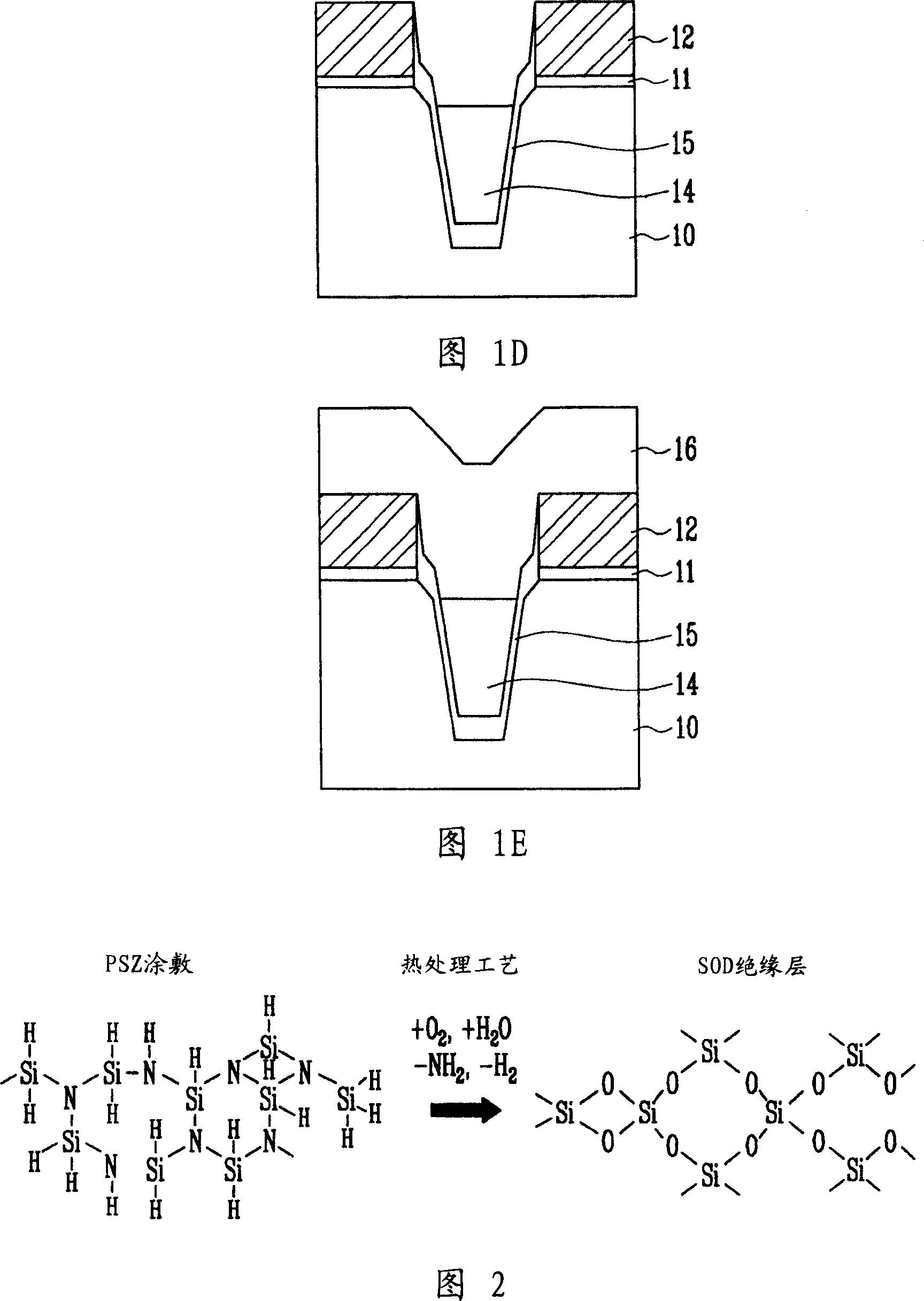
[0012] 1A to 1E are cross-sectional views of a semiconductor device for illustrating a method for forming an isolation structure of a semiconductor device according to an embodiment of the present invention. The accompanying drawings show embodiments of the present invention applied to a self-aligned shallow trench isolation (SA-STI) structure.

[0013] As shown in FIG. 1A, the tunnel oxide layer 11 and the polysilicon layer 12 for the floating gate are sequentially formed on the semiconductor substrate 10. By photolithography, the polysilicon layer 12 for the floating gate, the tunnel The through-oxide layer 11 and the semiconductor substrate 10 are etched to a specific depth to form isolation trenches 13 . Then, a first insulating layer 14 is formed on the surface including the isolation trench 13 . A high density plasma (HDP) oxide layer having a thickness of 100 to 2000 angstroms (A) is preferably formed as the first insulating layer 14 . The first insulating layer 14 is...


PUM


Abstract

A method for forming an isolation structure of a semiconductor device includes forming an isolation trench on a semiconductor substrate. A first insulating layer is formed over the isolation trench and the substrate. A spin-on-dielectric (SOD) insulating layer is formed over the first insulation layer, the SOD insulating layer filling the isolation trench and extending above an upper level of the isolation trench. The SOD insulating layer provided within the isolation trench is removed to expose an upper portion of the isolation trench, wherein a lower portion of the isolation trench remains filled with the SOD insulating layer. A second insulating layer is formed over the SOD insulating layer that is filling the lower portion of the isolation trench, wherein the second insulating layer fills the upper portion of the isolation trench.

Description

technical field [0001] The present invention relates to a method of forming an isolation structure of a semiconductor device, and more particularly to a method capable of improving the gap fill margin of a trench used for the isolation structure. Background technique [0002] In general, a semiconductor device includes isolation regions for electrically isolating respective circuit patterns. As semiconductor devices become more highly integrated and miniaturized, since the size of an active region and the process margin of a subsequent process depend on an isolation region formed in an initial step, studies for reducing the size of an isolation region have been actively studied. [0003] As semiconductor devices become more highly integrated and miniaturized, the LOCOS isolation method, which has previously been widely used to manufacture semiconductor devices, has largely been eliminated because the LOCOS method requires more space to perform than the Shallow Trench Isolati...

Claims


Application Information

Patent Timeline
Patent Type & Authority Applications(China)
IPC IPC(8): H01L21/762
CPCH01L21/76232Y02E50/10Y02E50/30C10B53/02C10B47/10C10L5/445
Inventor 金相德朴宝旻
Owner SK HYNIX INC
Features
  • R&D
  • Intellectual Property
  • Life Sciences
  • Materials
  • Tech Scout
  • Unparalleled Data Quality
  • Higher Quality Content
  • 60% Fewer Hallucinations
Learn More