Display device

A technology of display device and display area, applied in static indicators, instruments, nonlinear optics, etc., can solve the problem of increasing the frame area, and achieve the effect of reducing the frame area

Inactive Publication Date: 2007-11-28
ORTUS TECH
View PDF1 Cites 26 Cited by
  • Summary
  • Abstract
  • Description
  • Claims
  • Application Information

AI Technical Summary

Problems solved by technology

[0003] However, in the above-mentioned existing liquid crystal display device, since the electrostatic protection lines for scanning lines and the thin film transistors for electrostatic protection for scanning lines, the electrostatic protection lines for data lines and the thin films for electrostatic protection for data lines are arranged outside the display area Transistors, so in order to secure their configuration area, there is a problem of increased border area

Method used


Image

  • Display device
  • Display device
  • Display device

Examples


no. 1 approach

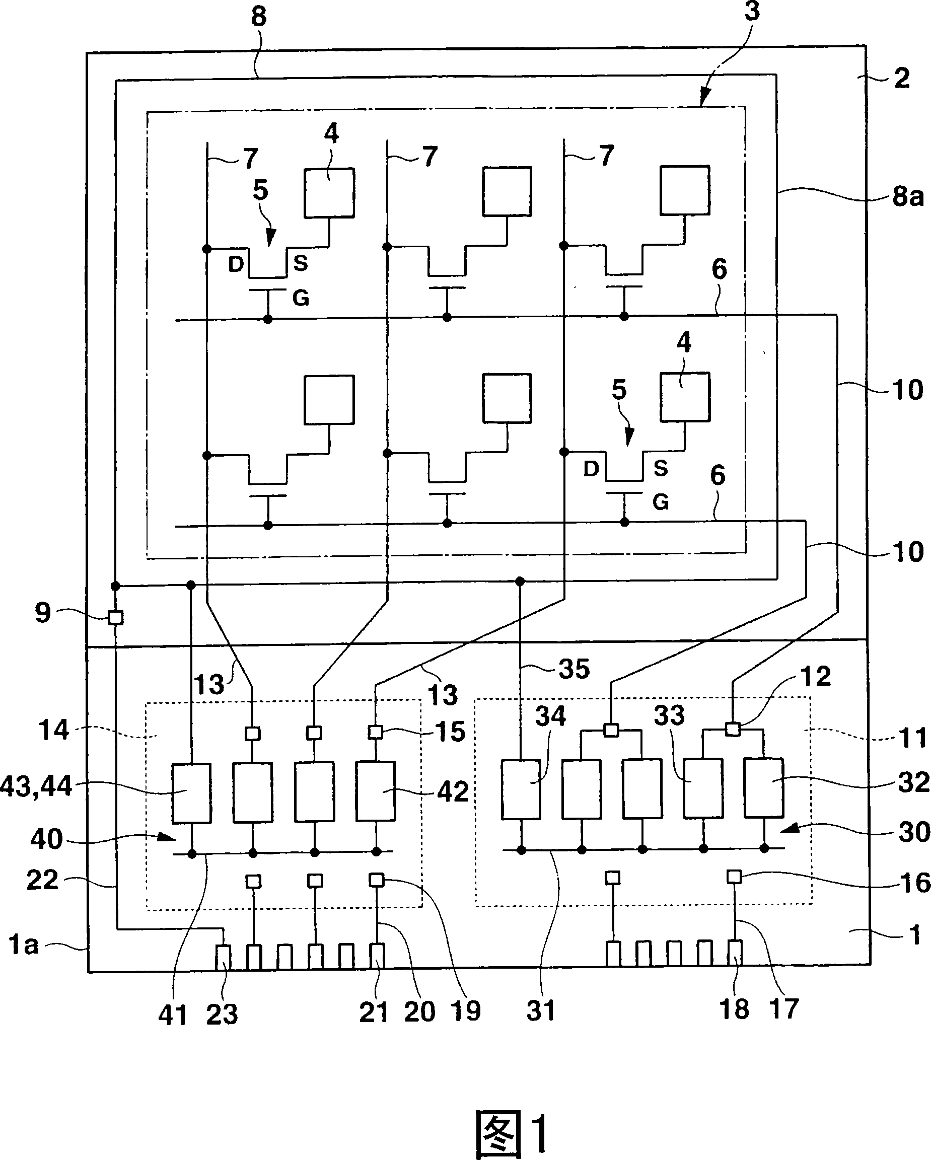
[0022] FIG. 1 is a plan view showing an equivalent circuit of main parts of a liquid crystal display device according to a first embodiment of the present invention. In this liquid crystal display device, the active substrate 1 and the opposite substrate 2 located above the active substrate 1 are bonded together by a substantially square-shaped sealing member (not shown), and the liquid crystal (not shown) is sealed in the sealing Between the two substrates 1 and 2 inside the component. At this time, the lower portion of the active substrate 1 protrudes from the counter substrate 2 . Hereinafter, this protruding portion is referred to as a protruding portion 1a. Moreover, the rectangular area enclosed by the dotted line in FIG. 1 is the display area 3 .

[0023] The display area 3 on the active substrate 1 is provided with: a plurality of pixel electrodes 4 arranged in a matrix, nMOS switching thin film transistors 5 having source electrodes S connected to each pixel electro...

no. 2 approach

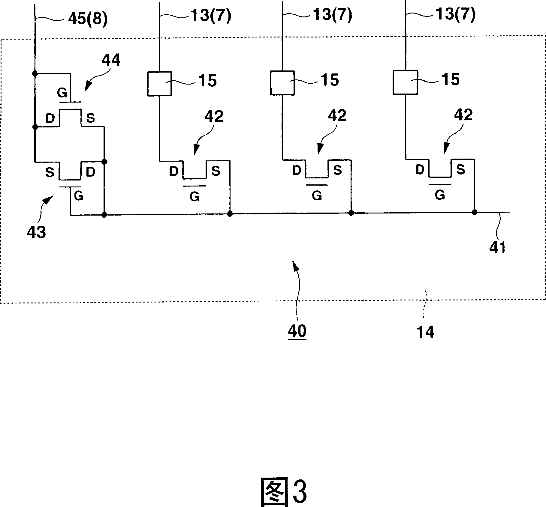
[0067] FIG. 9 is a cross-sectional view similar to FIG. 7 of a liquid crystal display device according to a second embodiment of the present invention. In this liquid crystal display device, the source electrode S of the data line electrostatic protection thin film transistor 42 is connected to the data line electrostatic protection line 41 provided on the upper surface of the gate insulating film 51 . Therefore, the contact hole 63 shown in FIG. 7 becomes unnecessary, and the interlayer contact portion can be further reduced.

[0068] In addition, in the liquid crystal display device of the second embodiment, as shown in FIG. 10 which is the same cross-sectional view as FIG. The source electrode S of the first connecting thin film transistor 43 and the drain electrode D of the second connecting thin film transistor 44 are connected to the contact hole 64 on the common lead 45, and the electrostatic protection line 41 is used to connect the data line to the second contact hole...

no. 3 approach

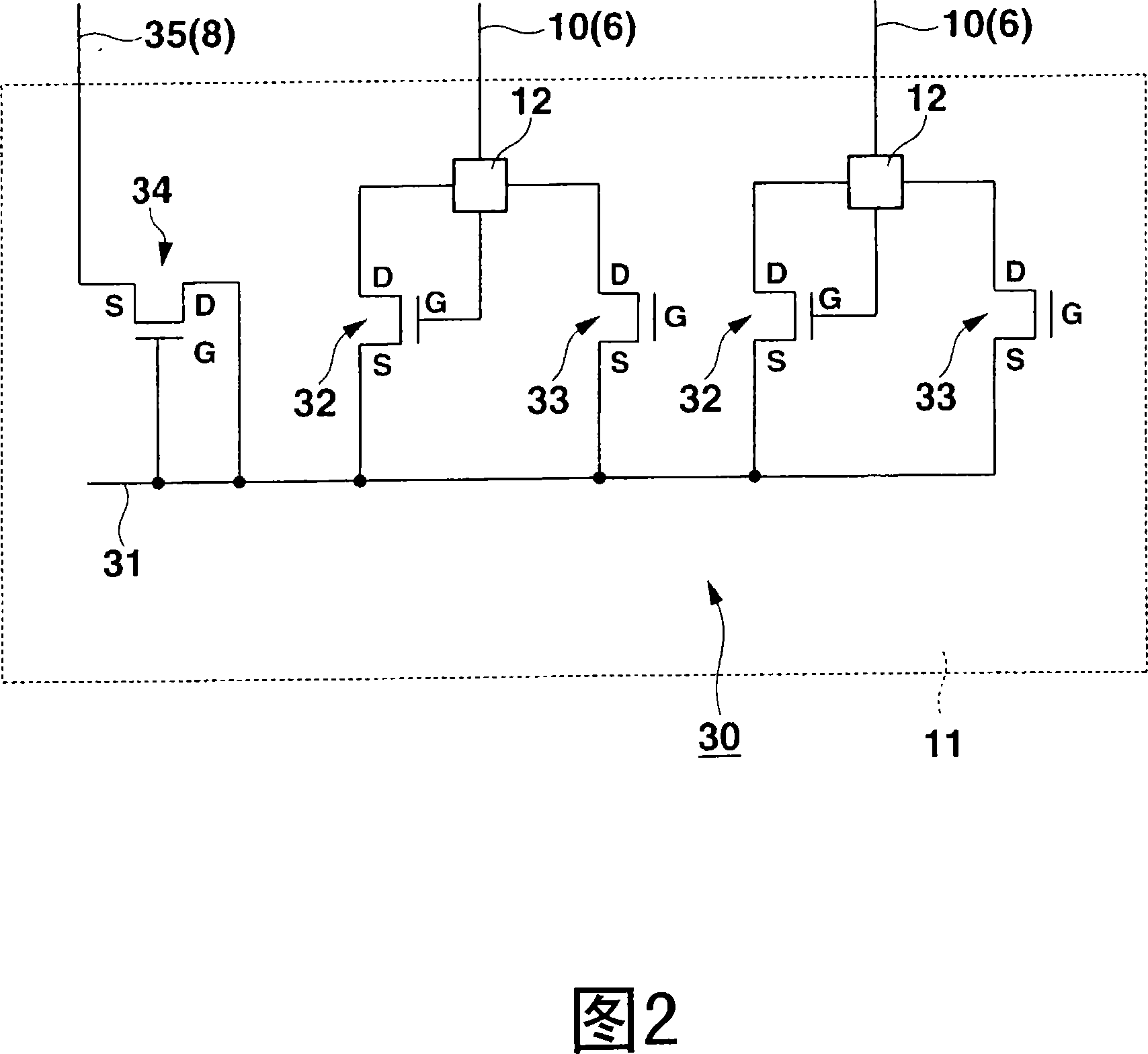
[0070] FIG. 11 is a plan view of an equivalent circuit similar to FIG. 2 of a liquid crystal display device according to a third embodiment of the present invention. In this liquid crystal display device, the difference from the structure shown in FIG. 2 is that the thin-film transistor 33 for static electricity protection for the second scanning line is omitted, and the source electrode S of the thin-film transistor 34 for connection is connected to the thin-film transistor 33 for driving the scanning line. On the Vgl terminal 71 in the driver mounting area 11.

[0071] At this time, a negative voltage (for example, Vgl=-20 to -15V) applied to the scanning line 6 in the non-selected state is supplied to the Vgl terminal 71 . The potential Vgl (-20 to -15V) of the scanning line 6 in the non-selected state is lower than the potential of the common line 8 (for example, Vcom=-5 to +5V). Therefore, a current flows from the electrostatic protection line 31 for scanning lines to th...


PUM


Abstract

The invention provides a display device that can reduce frame area. The display device comprises a substrate (1) that has a display region (3) and a non-display region, and a plurality of pixel electrodes (4) that are arranged in a matrix shape, display elements that are arranged correspondingly to each of the pixel electrodes (4), sistors (5) that are connected with each of the pixel electrodes (4) and used as switches are formed inside the display region (3) on the substrate (1); furthermore, each of the sistors (5) used as switches is connected with a scanning wire (6) that supplies scanning signals and a data wire (7) that supplies data signals. The non-display region of the substrate (1) comprises driver installation regions (11 and 14) for arranging drivers that are used for driving at least one of the scanning wire (6) and the data wire (7), and the driver installation regions (11 and 14) are provided with electrostatic protection circuits (30 and 40).

Description

technical field [0001] The invention relates to a display device with an electrostatic protection circuit. Background technique [0002] For example, in the existing active matrix liquid crystal display device, it has the following structure: in order to prevent the characteristics deviation and insulation breakdown caused by the static electricity of the switching thin film transistor, static electricity for scanning lines is provided outside the display area. The protective line and the thin film transistor for static electricity protection for the scanning line arranged between each scanning line and the static electricity protection line for the scanning line, the above-mentioned display area is provided near each intersection of a plurality of scanning lines and a plurality of data lines arranged in a matrix shape A pixel electrode and a switching thin film transistor connected to the pixel electrode are provided (for example, refer to Patent Document 1). [0003] Howe...

Claims


Application Information

Patent Timeline
Patent Type & Authority Applications(China)
IPC IPC(8): G02F1/1362G02F1/133
Inventor 中村弥生
Owner ORTUS TECH
Why Eureka
Try Eureka