X-ray sensor and fabrication method thereof

A manufacturing method and sensor technology, applied in semiconductor/solid-state device manufacturing, radiation control devices, instruments for radiological diagnosis, etc., can solve the problem of low data acquisition rate of X-ray sensors, and achieve the effect of improving the data acquisition rate

Active Publication Date: 2010-12-29
SHANGHAI TIANMA MICRO ELECTRONICS CO LTD
View PDF1 Cites 15 Cited by
  • Summary
  • Abstract
  • Description
  • Claims
  • Application Information

AI Technical Summary

Problems solved by technology

[0011] The purpose of the present invention is to provide a kind of X-ray sensor and manufac...

Method used


Image

  • X-ray sensor and fabrication method thereof
  • X-ray sensor and fabrication method thereof
  • X-ray sensor and fabrication method thereof

Examples


Embodiment Construction

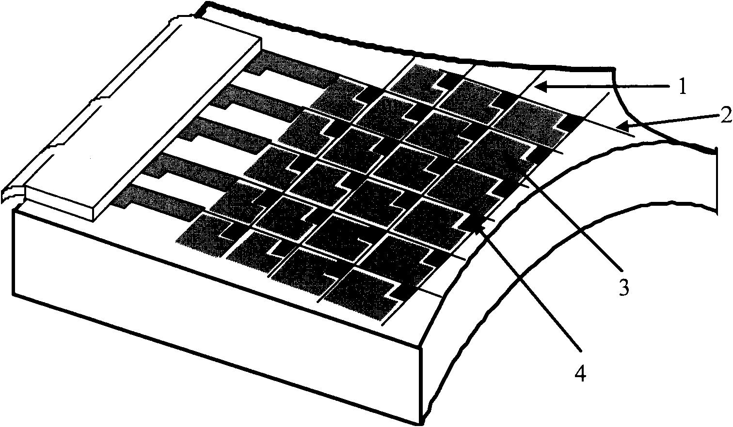
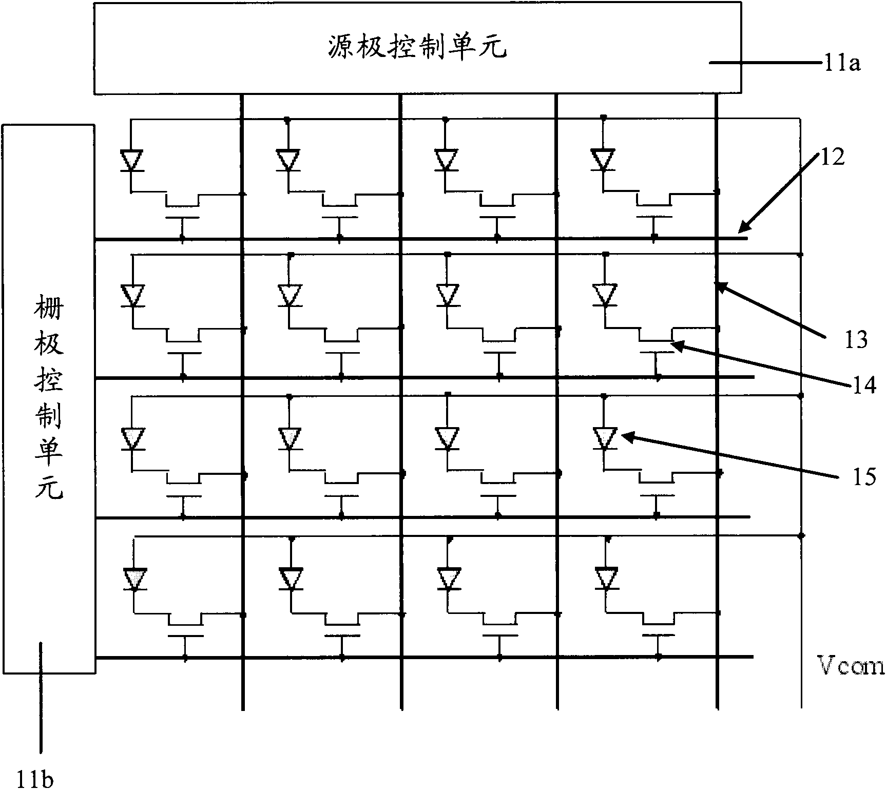
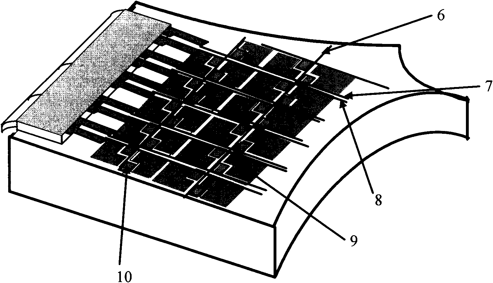
[0033] Aiming at the problem that the prior art X-ray sensor adopts a single-line scanning mode, which leads to a low data acquisition rate, the present invention provides an X-ray sensor, which realizes The working mode of multi-line scanning is used to improve the data acquisition rate of the X-ray sensor.

[0034] refer to image 3 As shown, an embodiment of the X-ray sensor of the present invention includes: an array of pixel units, wherein each pixel unit is composed of a photodiode 9 and a field effect transistor 10 . There are two data lines 7 and 8 between two adjacent columns of pixel units, and one scanning line 6 between two adjacent rows of pixel units. The field effect transistors in the two adjacent rows of pixel units share the same scan line, and the field effect transistors in each row of pixel units and the field effect transistors in the adjacent pixel units are respectively connected to different adjacent data lines. For example, the field effect transist...


PUM


Abstract

The invention relates to an X-ray sensor and a fabrication method thereof. The X-ray sensor comprises scanning lines, data lines and a pixel unit array, wherein the scanning lines and the data lines are arranged in a cross way, the pixel unit array is formed by the separation of the scanning lines and the data lines, each pixel unit comprises a switch element and a photoelectric sensing element connected with the switch element, at least two data lines are arranged between every two adjacent rows of pixel units, one scanning line is shared by at least two lines of pixel units, and in the at least two lines of pixel units, the switch elements of the pixel units in the same row are respectively connected with different data lines. The X-ray senor improves data acquisition rate and ensures that the quantity of the scanning lines is reduced by half, thereby correspondingly reducing the quantity of the driving circuits for driving the scanning lines.

Description

technical field [0001] The invention relates to the technical field of digital images, in particular to an X-ray sensor and a manufacturing method. Background technique [0002] With the development of society and the continuous progress of science and technology, various digital imaging medical technologies emerge in an endless stream, and digital imaging technology has played a very important role in today's medical field. In most of the existing digital imaging medical applications, such as X-ray chest X-ray, CT-computed tomography, the most important component for digital imaging technology is the X-ray (X-ray) sensor. [0003] figure 1 It is a schematic diagram of the structure of a flat-panel X-ray sensor. refer to figure 1 As shown, each pixel unit of the flat panel X-ray sensor is composed of a photodiode 3 and a field effect transistor (FET, Field Effect Transistor) 4 . Each field effect transistor is connected to an adjacent gate scanning line 1 , and each phot...

Claims


Application Information

Patent Timeline
IPC IPC(8): G01T1/00H01L27/146H01L21/82A61B6/02
Inventor 于祥国邱承彬孔杰李懿馨祁刚王婷
Owner SHANGHAI TIANMA MICRO ELECTRONICS CO LTD
Why Eureka
Try Eureka