Device and method for heating adhesive film used for bonding chips

A technology of heating device and heating method, which is applied in the fields of electrical components, semiconductor/solid-state device manufacturing, circuits, etc., and can solve the problems of damaging the active surface and reducing the packaging yield rate, etc.

Inactive Publication Date: 2011-05-11
ASE ASSEMBLY & TEST SHANGHAI
View PDF0 Cites 9 Cited by
  • Summary
  • Abstract
  • Description
  • Claims
  • Application Information

AI Technical Summary

Problems solved by technology

As a result, it was necessary to stop the production line to rule out accidental sticking problems
Furthermore, the vacuum pick-and-place head 13 needs to make its suction head with metal material because it needs to conduct heat ...

Method used


Image

  • Device and method for heating adhesive film used for bonding chips
  • Device and method for heating adhesive film used for bonding chips
  • Device and method for heating adhesive film used for bonding chips

Examples


Embodiment Construction

[0026] In order to make the above-mentioned purposes, features and advantages of the present invention more obvious and understandable, the preferred embodiments of the present invention will be specifically cited below, together with the accompanying drawings, for a detailed description as follows:

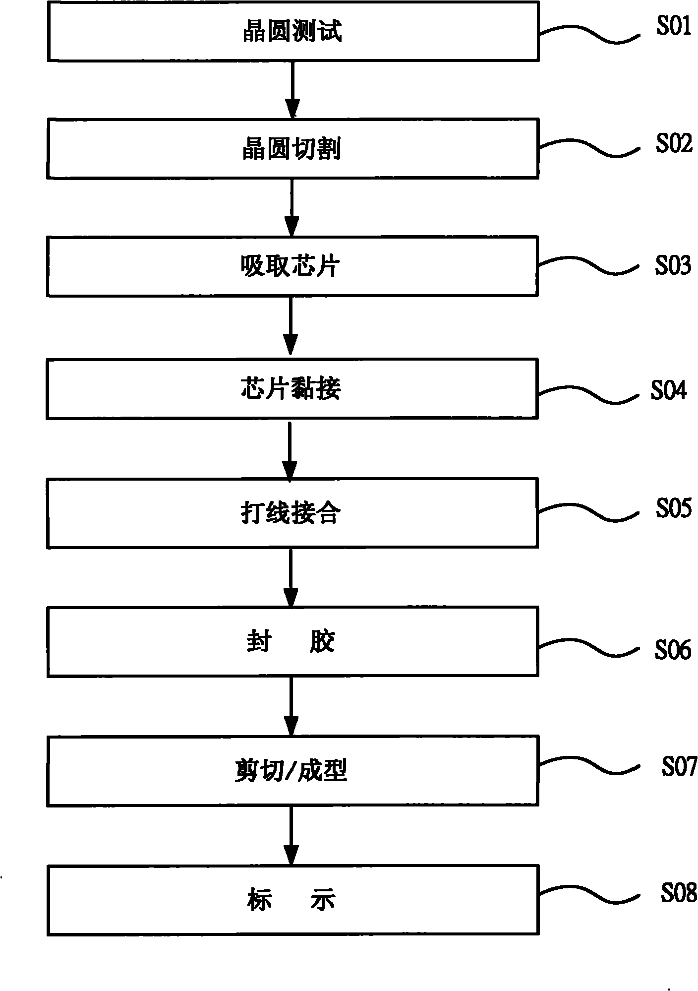
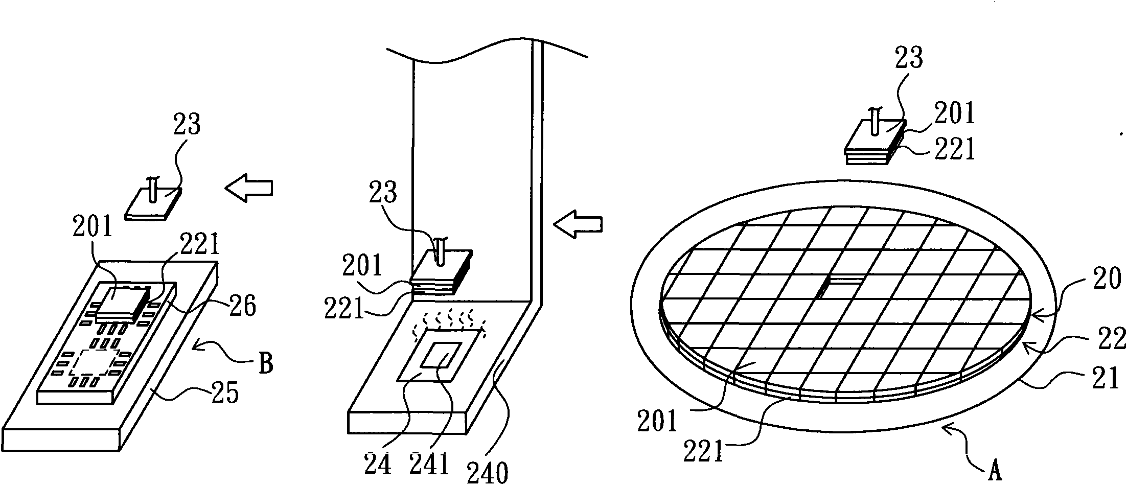
[0027] Please refer to image 3 As shown, the heating device and method of the die bonding adhesive film of the first embodiment of the present invention are mainly used in similar figure 1In the semiconductor chip wire bonding process shown in the chip suction step S03 and the die bonding step S04. The heating device for the adhesive film for die bonding according to the first embodiment of the present invention is mainly located between a chip suction position A and a chip bonding position B, and the chip suction position A uses a wafer fixing adhesive film 21 to carry a A semiconductor chip 20 and an adhesive film 22 for die bonding. The heating device mainly includes a chip...


PUM


Abstract

The invention discloses a device and a method for heating an adhesive film used for bonding chips. The adhesive film used for bonding semiconductor chips sucked by a chip picking and placing head on the moving path of the chip picking and placing head is subjected to non-contact heating in a fixed point mode or a synchronous moving mode through a non-contact heating unit, so that the time required for heating and softening the adhesive film and the time required for bonding the chips can be shortened, the efficiency for bonding the chips are improved and the yield of an encapsulated product within unit time is increased; the adhesive film can be prevented from being heated and softened prematurely, so that the adhesive film is prevented from sticking an adhesive film used for bonding wafers or sticking adjacent chips and adhesive films at the sucking positions of the chips unexpectedly; therefore, unexpected bonding problems are effectively solved and the reliability of production line operation is improved.

Description

【Technical field】 [0001] The present invention relates to a heating device and method for an adhesive film for chip bonding, in particular to a device for non-contact heating of the adhesive film for chip bonding between the chip suction step and the chip bonding step Heating device and method thereof. 【Background technique】 [0002] In the manufacturing process of the semiconductor package structure, wire bonding technology has been widely used in the electrical connection between the semiconductor chip and the package substrate (substrate) or leadframe (leadframe). Please refer to figure 1 As shown, it outlines the main processing steps included in the existing semiconductor chip bonding process, which generally includes: a wafer test (wafer test) step S01, wherein a semiconductor wafer is tested by using several probes of a test machine Whether the circuit block on the round surface is good, and obtain the information of the good product block and the defective product ...

Claims


Application Information

Patent Timeline
IPC IPC(8): H01L21/00H01L21/50
Inventor 史海涛周若愚
Owner ASE ASSEMBLY & TEST SHANGHAI
Why Eureka
Try Eureka