

Method for forming NMOS (N-channel Metal Oxide Semiconductor) transistor
A technology of transistors and barrier layers, applied in the fields of semiconductor devices, semiconductor/solid-state device manufacturing, electrical components, etc., can solve the problems of NMOS transistor threshold voltage drop and other problems, and achieve the effect of improving reliability
- Summary
- Abstract
- Description
- Claims
- Application Information
AI Technical Summary
Problems solved by technology
Method used
Image

Examples
Embodiment Construction
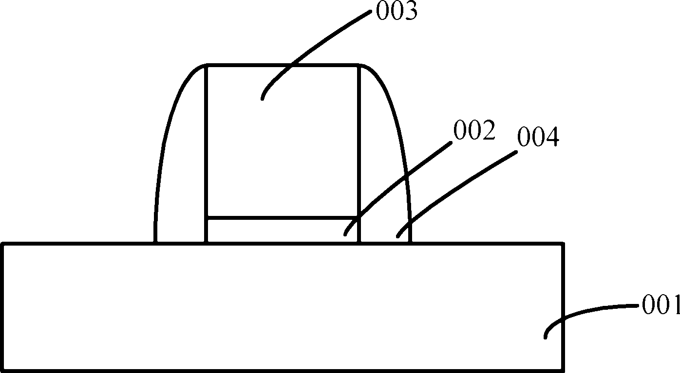
[0034] The prior art uses stress memorization techniques (SMT) to increase the compressive stress in the vertical direction of the channel region, but the threshold voltage of the NMOS transistor formed by the method is significantly higher than the standard threshold voltage value to be formed. decline.
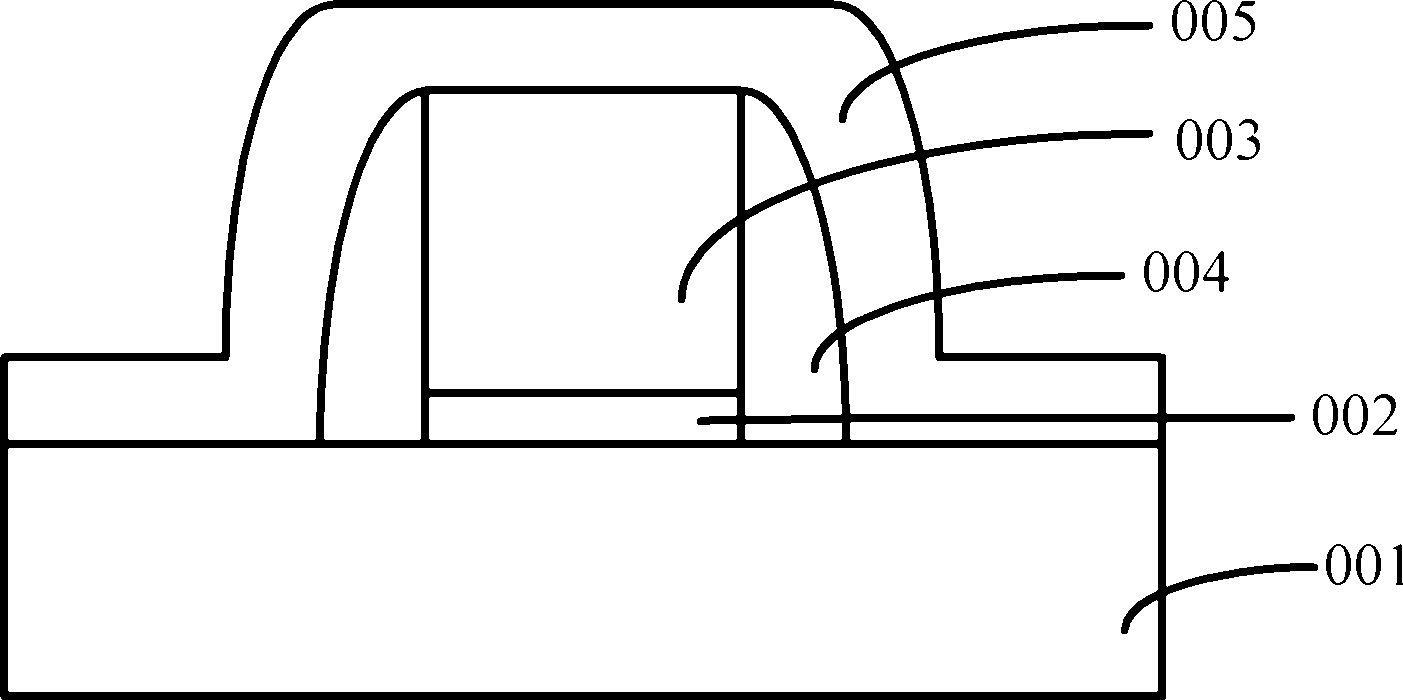
[0035] refer to figure 1 and to figure 2 The inventors found that after the stress layer 005 was formed, the concentration of dopant ions in the source / drain region decreased more than the concentration of dopant ions before the formation of the stress layer 005, which reduced the difficulty of opening the channel region, In turn, the threshold voltage and the standard threshold voltage to be formed are significantly lowered.
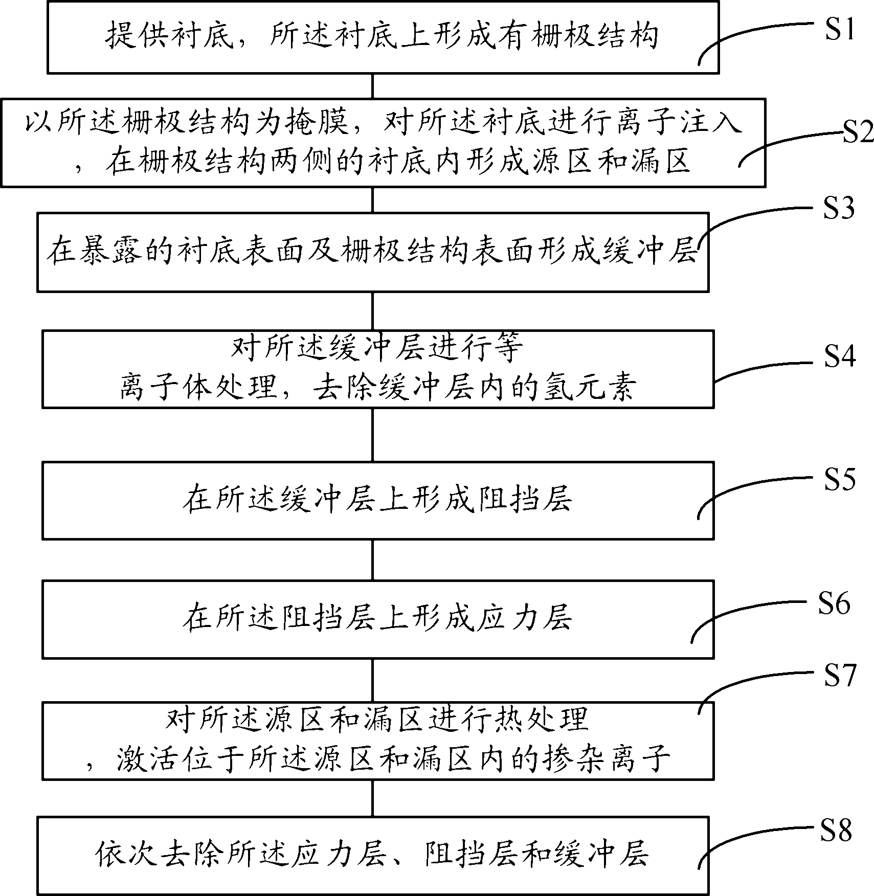
[0036] The inventors further found that the process environment for forming the stress layer 005 will cause the formed stress layer 005 to contain hydrogen. For example, when the chemical vapor deposition method is used to form the stress layer 00...
PUM
 Abstract
Description
Claims
Application Information