Supercharge Your Innovation With Domain-Expert AI Agents!

Illumination system of projection exposure device for microlithography

A lighting system and exposure device technology, applied in the field of lighting systems, can solve problems such as the uniformity of spatial and angular irradiance distribution, and achieve the effect of reducing field dependence

Active Publication Date: 2015-08-19
CARL ZEISS SMT GMBH
View PDF11 Cites 0 Cited by
  • Summary
  • Abstract
  • Description
  • Claims
  • Application Information

AI Technical Summary

Problems solved by technology

[0011] While illumination systems using mirror arrays are very flexible for modifying the angular irradiance distribution, the uniformity of the spatial and angular irradiance distribution over the illumination field in the mask plane remains an issue

Method used


Image

  • Illumination system of projection exposure device for microlithography
  • Illumination system of projection exposure device for microlithography
  • Illumination system of projection exposure device for microlithography

Examples


Embodiment Construction

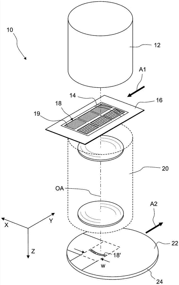
[0105] I. Overall structure of the projection exposure device

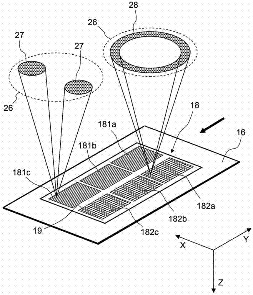
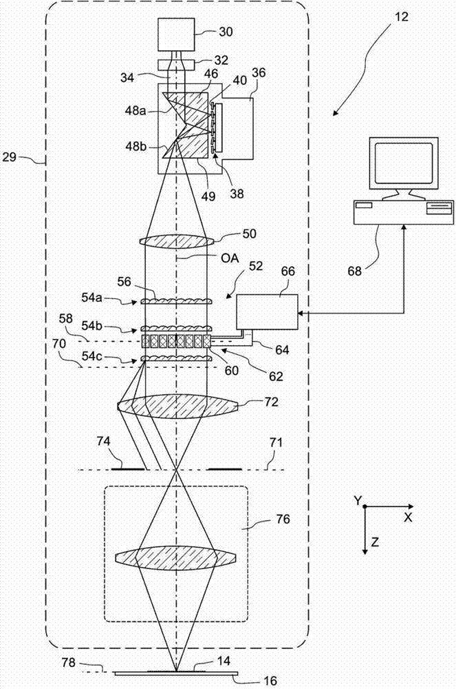
[0106] figure 1 is a perspective and highly simplified view of a projection exposure apparatus 10 according to the invention. Apparatus 10 includes an illumination system 12 that generates a projected light beam. The projected beam illuminates a field 14 on a mask 16 containing figure 1 A pattern 18 is formed of a plurality of small features 19 schematically represented by thin lines in the middle. In this embodiment, the field of illumination 14 has the shape of a ring segment that does not contain the optical axis OA of the device. However, illumination fields 14 of other shapes are also conceivable, for example rectangular.

[0107] Projection objective 20 images pattern 18 within illuminated field 14 onto a photosensitive layer 22 (eg, photoresist) supported by substrate 24 . A substrate 24 , which may be formed from a silicon wafer, is arranged on a wafer stage (not shown in the figure) such that the top...


PUM


Abstract

An illumination system of a microlithographic projection exposure apparatus includes an optical integrator that includes an array of optical raster elements. A condenser superimposes the light beams associated with the optical raster elements in a common field plane. A modulator modifies a field dependency of an angular irradiance distribution in an illuminated field. Units of the modulator are associated with one of the light beams and are arranged at a position in front of the condenser such that only the associated light beam impinges on a single modulator unit. The units are configured to variably redistribute, without blocking any light, a spatial and / or an angular irradiance distribution of the associated light beams. A control device controls the modulator units if it receives an input command that the field dependency of the angular irradiance distribution in the mask plane shall be modified.

Description

technical field [0001] The present invention generally relates to an illumination system of a projection exposure apparatus for microlithography and to a method of operating such an apparatus. Background technique [0002] Microlithography (also known as photolithography, lithography) is a technique used to fabricate integrated circuits, liquid crystal displays, and other microstructured devices. Microlithography processes are used in conjunction with etching processes to pattern features in thin film stacks that have been formed on a substrate such as a silicon wafer. At each layer of fabrication, the wafer is first coated with photoresist, a material that is sensitive to specific wavelengths of light. Next, the wafer with photoresist on top is exposed to projected light through a mask in a projection exposure apparatus. The mask contains the circuit pattern to be imaged on the photoresist. After exposure, the photoresist is developed to produce an image corresponding to...

Claims


Application Information

Patent Timeline
Patent Type & Authority Patents(China)
IPC IPC(8): G03F7/20
CPCG03F7/70116G03F7/70191G03F7/70091G03F7/20
Inventor M.帕特拉M.施瓦布
Owner CARL ZEISS SMT GMBH
Features
  • R&D
  • Intellectual Property
  • Life Sciences
  • Materials
  • Tech Scout
  • Unparalleled Data Quality
  • Higher Quality Content
  • 60% Fewer Hallucinations
Learn More