Printed circuit board processing method, printed circuit board and electronic device

A processing method and technology of printed circuit boards, which are applied in the directions of printed circuit components, electrical connection formation of printed components, electrical connection of printed components, etc., can solve problems such as open circuit, unstable high-frequency signal transmission performance, poor reliability, etc.

Active Publication Date: 2014-01-15
SHENNAN CIRCUITS
View PDF7 Cites 14 Cited by
  • Summary
  • Abstract
  • Description
  • Claims
  • Application Information

AI Technical Summary

Problems solved by technology

Practice has found that although the existing connection method connects the ground layer and the metal base, the reliability of this c

Method used


Image

  • Printed circuit board processing method, printed circuit board and electronic device
  • Printed circuit board processing method, printed circuit board and electronic device
  • Printed circuit board processing method, printed circuit board and electronic device

Examples


Embodiment Construction

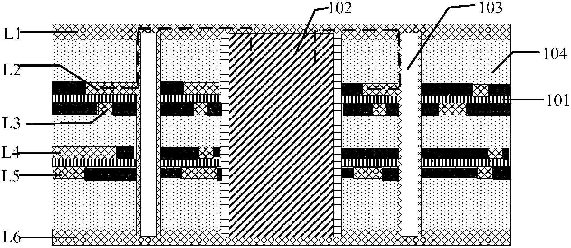
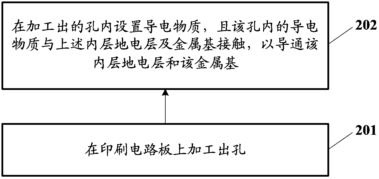
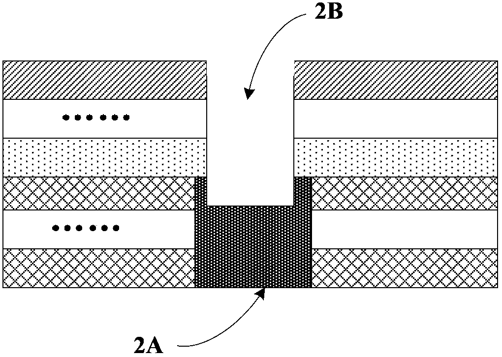
[0077] Embodiments of the present invention provide a PCB processing method, a printed circuit board, and electronic equipment, in order to improve the reliability of the connection between the inner ground layer of the PCB and the metal base, and improve the transmission performance of high-frequency signals.

[0078] In order to enable those skilled in the art to better understand the solutions of the present invention, the following will clearly and completely describe the technical solutions in the embodiments of the present invention in conjunction with the drawings in the embodiments of the present invention. Obviously, the described embodiments are only It is an embodiment of a part of the present invention, but not all embodiments. Based on the embodiments of the present invention, all other embodiments obtained by persons of ordinary skill in the art without making creative efforts shall fall within the protection scope of the present invention.

[0079] see first fi...


PUM


Abstract

Embodiments of the invention discloses a PCB (printed circuit board), a PCB processing method and an electronic device. The PCB processing method can comprise: processing a hole on the PCB, wherein the PCB comprises a metal base and at least two layers of base materials, at least one layer of base material from the at least two layers of base materials being provided with a geoelectrical layer thereon and the metal base being fixedly arranged in a groove provided on the base materials, and the processed hole contacting both the geoelectrical layer and the metal base; and arranging a conductive substance in the hole, the conductive substance in the hole contacting the inner layer of the geoelectrical layer and the metal base so as to switch on the inner layer of the geoelectrical layer and the metal base. The scheme of the embodiments of the invention is favourable to improving the reliability of connection between the geoelectrical layer and the metal base of the PCB and improving the transmission performance of a high-frequency signal.

Description

technical field [0001] The invention relates to the field of printed circuit board manufacturing, in particular to a method for processing a printed circuit board, a printed circuit board and electronic equipment. Background technique [0002] At present, there are many types of printed circuit boards (PCB, Printed Circuit Board), and their application range is extremely wide. In high-frequency and high-speed PCBs, the metal base embedded in the PCB is mainly grounded through the conduction with the inner ground layer of the PCB. [0003] In the prior art, the metal base and the inner ground layer are connected through wires. Practice has found that although the existing connection method connects the ground layer and the metal base, the reliability of this connection method is poor, and it is often prone to disconnection; and the transmission performance of high-frequency signals is unstable. Contents of the invention [0004] Embodiments of the present invention provid...

Claims


Application Information

Patent Timeline
IPC IPC(8): H05K3/40H05K1/11
Inventor 李传智缪桦谢占昊彭军
Owner SHENNAN CIRCUITS
Why Eureka
Try Eureka