Method for processing groove on printed circuit board, printed circuit board and electronic device

A technology for printed circuit boards and processing slots, which is applied to printed circuits, printed circuit manufacturing, printed circuit components, etc. It can solve problems such as unfavorable product cost control and obstacles to PCB miniaturization and integration, and promote PCB miniaturization and high integration. The effect of shortening the processing cycle, reducing the overall volume and weight

Active Publication Date: 2014-01-15
WUXI SHENNAN CIRCUITS CO LTD
View PDF3 Cites 30 Cited by
  • Summary
  • Abstract
  • Description
  • Claims
  • Application Information

AI Technical Summary

Problems solved by technology

[0003] Practice has found that the existing cooling solutions for components hinder the

Method used


Image

  • Method for processing groove on printed circuit board, printed circuit board and electronic device
  • Method for processing groove on printed circuit board, printed circuit board and electronic device
  • Method for processing groove on printed circuit board, printed circuit board and electronic device

Examples


Embodiment Construction

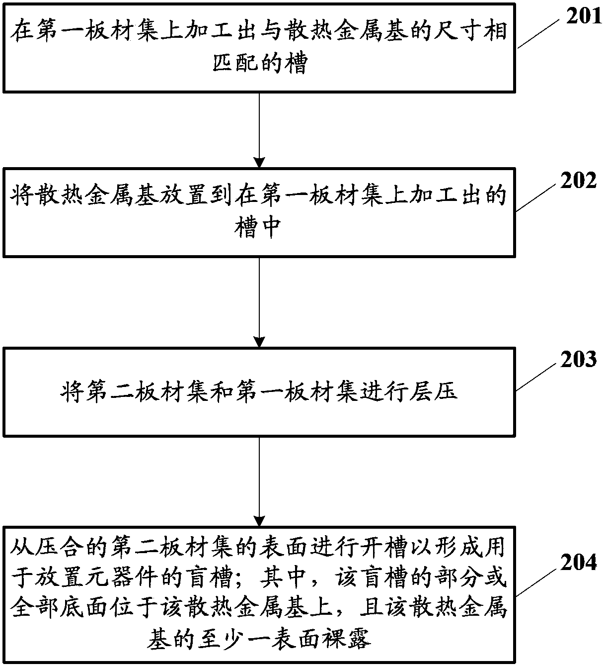
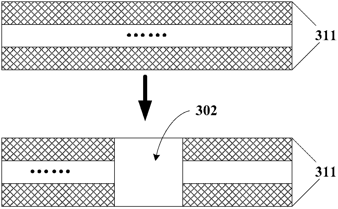
[0070] Embodiments of the present invention provide a method for processing grooves on a printed circuit board, the printed circuit board and electronic equipment, in order to promote product miniaturization and integration and cost control.

[0071] The following will clearly and completely describe the technical solutions in the embodiments of the present invention with reference to the accompanying drawings in the embodiments of the present invention. Obviously, the described embodiments are only some, not all, embodiments of the present invention. Based on the embodiments of the present invention, all other embodiments obtained by persons of ordinary skill in the art without creative efforts fall within the protection scope of the present invention.

[0072] The following describes in detail respectively through the examples.

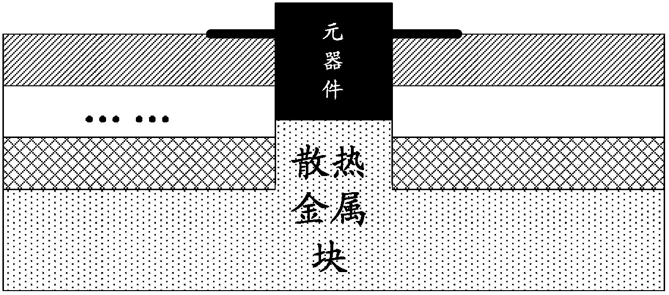
[0073] see figure 1 , figure 1 It is an example of a component heat dissipation structure of a common PCB, wherein a heat dissipation metal plate...


PUM


Abstract

Embodiments of the invention disclose a method for processing a groove on a printed circuit board, the printed circuit board and an electronic device. The method for processing the groove on the printed circuit board comprises: processing the groove, the dimension of which is matched with that of a heat-dissipating metal base on a first board set; fixedly arranging the heat-dissipating metal base in the groove processed in the first board set; stitching a second board set with the first board set and thus a third board set is formed; providing a groove in the surface of the second board set after stitching so as to form a blind groove for installing components, wherein partial or all bottom surface of the blind groove is arranged on the heat-dissipating metal base and at least one surface of the heat-dissipating metal base is exposed; and the depth of the blind groove in the vertical direction on the surface of the third board set is larger than the thickness of the second board set after stitching. The scheme provided in the embodiments of the invention is benefit to promote product miniaturization, integration and cost control.

Description

technical field [0001] The invention relates to the field of printed circuit board manufacturing, in particular to a method for processing grooves on the printed circuit board, the printed circuit board and electronic equipment. Background technique [0002] It is applied to high heating components such as power amplifiers (PA, Power Amplifier) ​​in many electronic devices. For example, PA is applied in high-power wireless base stations. The core of PA lies in matching design, heat dissipation design, linearity, consistency and efficiency, etc. Among them, except for matching, other characteristics are closely related to heat dissipation. Heat dissipation is a major factor affecting efficiency and linearity. Among the existing heat dissipation solutions for components, the heat dissipation metal-based printed circuit board (PCB, Printed Circuit Board) is a more effective solution. Among them, the existing heat dissipation metal-based PCB is used to carry PA or other compone...

Claims


Application Information

Patent Timeline
IPC IPC(8): H05K3/00H05K3/30H05K1/02
Inventor 李传智缪桦谢占昊
Owner WUXI SHENNAN CIRCUITS CO LTD
Why Eureka
Try Eureka