Pixel structure, manufacturing method thereof, array substrate of pixel structure and liquid crystal display panel of pixel structure

A pixel structure, array substrate technology, applied in nonlinear optics, instruments, optics, etc., can solve the problems of uneven display color, uneven color, etc., and achieve the effect of offsetting color distortion, displaying color uniformity, and wide viewing angle display.

Inactive Publication Date: 2014-01-22
HEFEI BOE OPTOELECTRONICS TECH +1
View PDF3 Cites 5 Cited by
  • Summary
  • Abstract
  • Description
  • Claims
  • Application Information

AI Technical Summary

Problems solved by technology

[0004] However, if figure 1 As shown, when the data signal voltage is input through the data line 2, the orientation of the liquid crystal molecules 10 is close to the horizontal direction. Therefore, for the IPS type liquid crystal display panel, only a wide viewing angle in the up and down direction can be formed. When the user views the IPS from the left and right directions When using a small LCD panel, there will be uneven col

Method used


Image

  • Pixel structure, manufacturing method thereof, array substrate of pixel structure and liquid crystal display panel of pixel structure
  • Pixel structure, manufacturing method thereof, array substrate of pixel structure and liquid crystal display panel of pixel structure
  • Pixel structure, manufacturing method thereof, array substrate of pixel structure and liquid crystal display panel of pixel structure

Examples


Example Embodiment

[0025] In order for those skilled in the art to better understand the technical solutions of the present invention, the pixel structure and its manufacturing method, array substrate and liquid crystal display panel provided by the present invention are described below with reference to the accompanying drawings. Describe in detail.

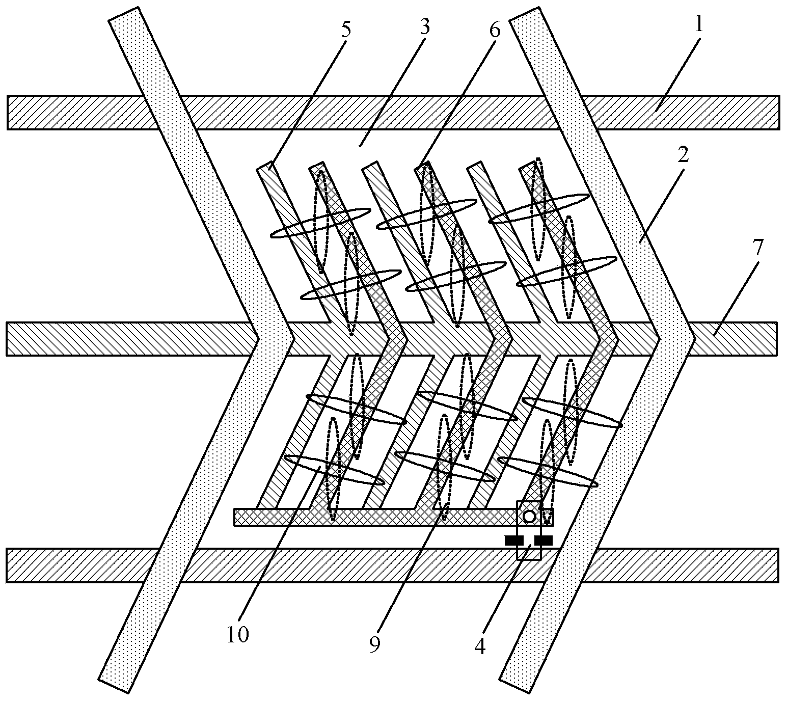
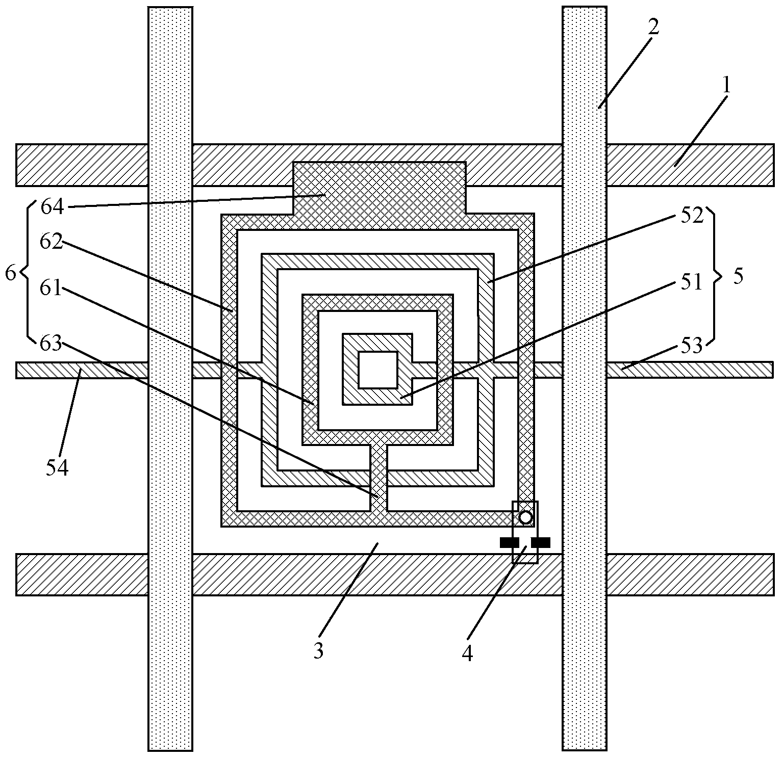
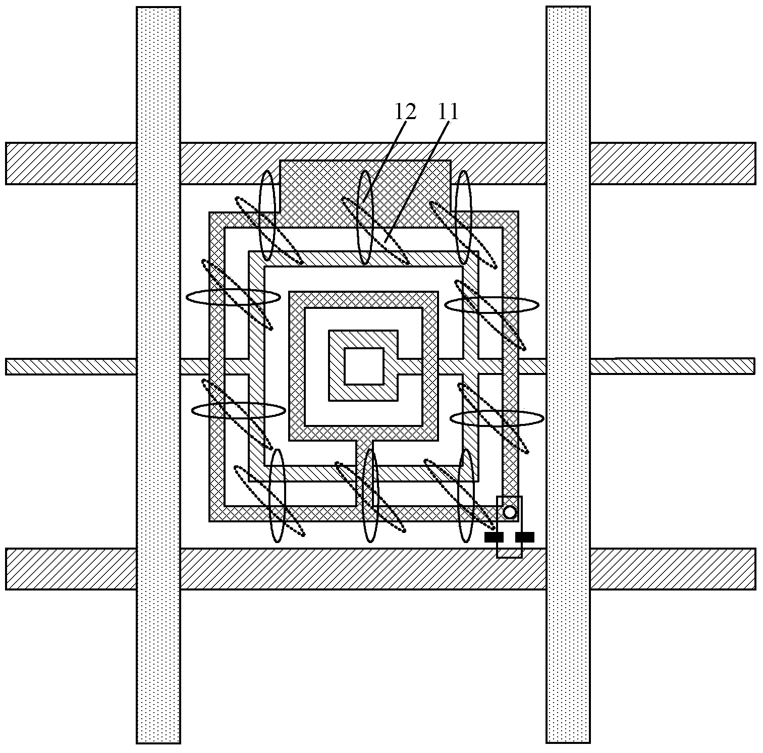
[0026] figure 2 A schematic structural diagram of a pixel structure provided in Embodiment 1 of the present invention, such as figure 2 As shown, the pixel structure includes: a gate line 1 and a data line 2, the gate line 1 and the data line 2 define a pixel unit 3, and the pixel unit 3 includes: a pixel driving unit 4, a common electrode 5 and a pixel electrode 6, and the pixel driving unit 4 It is electrically connected to the pixel electrode 6, the common electrode 5 includes at least one common electrode pattern, the pixel electrode 6 includes at least one pixel electrode pattern, the common electrode pattern and the pixel electrode patter...


PUM


Abstract

The invention discloses a pixel structure, a manufacturing method thereof, an array substrate of the pixel structure and a liquid crystal display panel of the pixel structure. The pixel structure comprises a grid line and a data line, wherein a pixel unit is limited by the grid line and the data line and comprises a pixel driving unit, a common electrode and a pixel electrode; the pixel driving unit is electrically connected with the pixel electrode; the common electrode comprises at least one common electrode graph; the pixel electrode comprises at least one pixel electrode graph; the common electrode graphs and the pixel electrode graphs are nested to one another and are arranged at intervals; and an electric field for deflection of liquid crystal molecules is formed between the common electrode graphs and the pixel electrode graphs adjacent to the common electrode graphs. According to the technical scheme, wide viewing-angle displaying in the four directions is realized, displaying colors in the four directions are uniform, color aberrations can be well counteracted, and color purity is improved.

Description

technical field [0001] The invention relates to the field of display technology, in particular to a pixel structure and a manufacturing method thereof, an array substrate and a liquid crystal display panel. Background technique [0002] A liquid crystal display panel (Liquid Crystal Display, LCD for short) displays images by selectively changing the light transmittance of a liquid crystal disposed between an upper substrate and a lower substrate. According to the direction of the electric field applied to the liquid crystal, the liquid crystal display panel can be roughly classified into a vertical electric field application type liquid crystal display panel and a horizontal electric field application type liquid crystal display panel. [0003] Generally, a twisted nematic (TN) type liquid crystal display panel is a vertical electric field application type liquid crystal display panel. In a TN type liquid crystal display panel, between the pixel electrodes formed on the lowe...

Claims


Application Information

Patent Timeline
IPC IPC(8): G02F1/1343G02F1/1337
Inventor 刘国冬胡明
Owner HEFEI BOE OPTOELECTRONICS TECH
Why Eureka
Try Eureka