OLED pixel arrangement structure and display device

A technology for pixel arrangement and display device, applied in electrical components, electric solid devices, circuits, etc., can solve the problems of low pixel density and PPI cannot be greatly improved, achieve uniform display color, improve PPI value and resolution, improve Image quality and effects of effects

Active Publication Date: 2017-12-22
TRULY HUIZHOU SMART DISPLAY
View PDF3 Cites 0 Cited by
  • Summary
  • Abstract
  • Description
  • Claims
  • Application Information

AI Technical Summary

Problems solved by technology

[0004] The main factor affecting the high PPI value is the high fineness of the mask plate. Since the mask plate (Mask) opening area has a lower limit of specification, and in order to avoid the influence of the tolerance (tolerance) in the manufacturing process, the openings of adjacent pixels need to be pre-set. Leaving a gap (gap) results in a small pixel density, resulting in the inability to greatly improve the PPI

Method used


Image

  • OLED pixel arrangement structure and display device
  • OLED pixel arrangement structure and display device
  • OLED pixel arrangement structure and display device

Examples


Embodiment Construction

[0022] In order to make the objectives, technical solutions and advantages of the present invention clearer, the following further describes the present invention in detail with reference to the accompanying drawings and embodiments. It should be understood that the specific embodiments described herein are only used to explain the present invention, but not to limit the present invention.

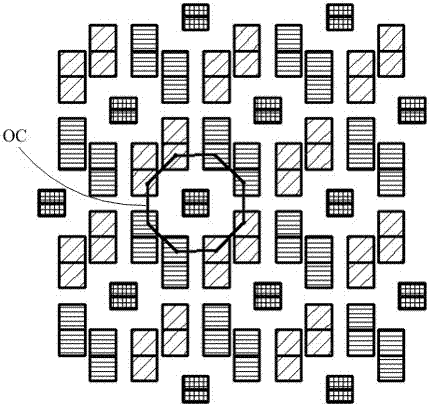
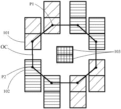
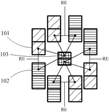
[0023] See figure 1 and figure 2 , The OLED pixel arrangement structure of the first embodiment of the present invention includes a plurality of first sub-pixels 101, second sub-pixels 102, and third sub-pixels 103 forming a repeated arrangement of virtual octagons OC, each virtual octagon OC Consists of four first sub-pixels 101, four second sub-pixels 102 and at least two third sub-pixels 103, the centers of the at least two third sub-pixels 103 coincide with the centers of the virtual octagon OC The centers of the four first sub-pixels 101 are respectively located at the four first vertic...


PUM


Abstract

The invention discloses an OLED (optical light emitting diode) pixel arrangement structure and a display device. The pixel arrangement structure comprises a plurality of repeated arrangement virtual octagons, wherein each virtual octagon consists of four first sub pixels, four second sub pixels and at least two third pixels, the centers of the at least two third sub pixels are coincident with the center of the virtual octagon, the centers of the four first sub pixels of each virtual octagon are respectively positioned at four first peaks of the left upper corner and the right lower corner of the virtual octagon, the centers of the four second sub pixels of each virtual octagon are respectively positioned on four second peaks of the right upper corner and the left lower corner of the virtual octagon, and a basic pixel unit is formed through the adjacent first sub pixels and the second sub pixels in each virtual octagon and the third sub pixels opposite to the first sub pixels and the second sub pixels. The OLED pixel arrangement structure and the display device have the advantages that the limitation of a manufacturing process and a film plating process is broken through, an OLED display PPI (pixels per inch) value and the resolution ratio can be effectively improved, and the OLED display image quality and the OLED display image effect are improved.

Description

Technical field [0001] The present invention relates to the technical field of semiconductor manufacturing, in particular to an OLED pixel arrangement structure and a display device. Background technique [0002] In recent years, organic light-emitting diodes (Organic Light-Emitting Diode, OLED) are self-luminous, do not need a backlight, and have high contrast, thin thickness, wide viewing angle, fast response speed, and can be used for flexible panels and operating temperature range. Wide, simple structure and manufacturing process and other excellent characteristics, are considered as the next generation of flat panel display emerging application technology. Organic light-emitting display technology is composed of very thin organic material coatings and glass substrates. When electric charges pass through, these organic materials emit light. Compared with LCD displays, OLED has the advantages of more power saving, thinner, and wide viewing angle, which is unmatched by LCD. O...

Claims


Application Information

Patent Timeline
Patent Type & Authority Patents(China)
IPC IPC(8): H01L27/32
Inventor 李志庆张亮邹新吴炜钦柯贤军苏君海黄亚清李建华
Owner TRULY HUIZHOU SMART DISPLAY
Why Eureka
Try Eureka