Structure of an optical interference display cell

a technology of optical interference and display cell, applied in the field of structure of optical interference display, can solve the problems of poor resolution, low yield, complicated manufacturing process, etc., and achieve the effect of high resolution and brightness of color optical interference display

Inactive Publication Date: 2005-04-19
SNAPTRACK
View PDF4 Cites 337 Cited by
  • Summary
  • Abstract
  • Description
  • Claims
  • Application Information

AI Technical Summary

Benefits of technology

[0010]It is therefore an objective of the present invention to provide an optical interference display unit structure used to form a color optical interference display. The resolution and brightness of the color optical interference display is high.

Problems solved by technology

One of the disadvantages of a multi-layered color planar display is its poor resolution.
The manufacturing process is complicated and the yield is low.
Moreover, the errors introduced during the manufacturing process, for instance, the errors of the lengths of cavities may cause red shift or blue shift.
The mistake is uncorrectable and the substrate is wasted.

Method used


Image

  • Structure of an optical interference display cell
  • Structure of an optical interference display cell
  • Structure of an optical interference display cell

Examples


embodiment 1

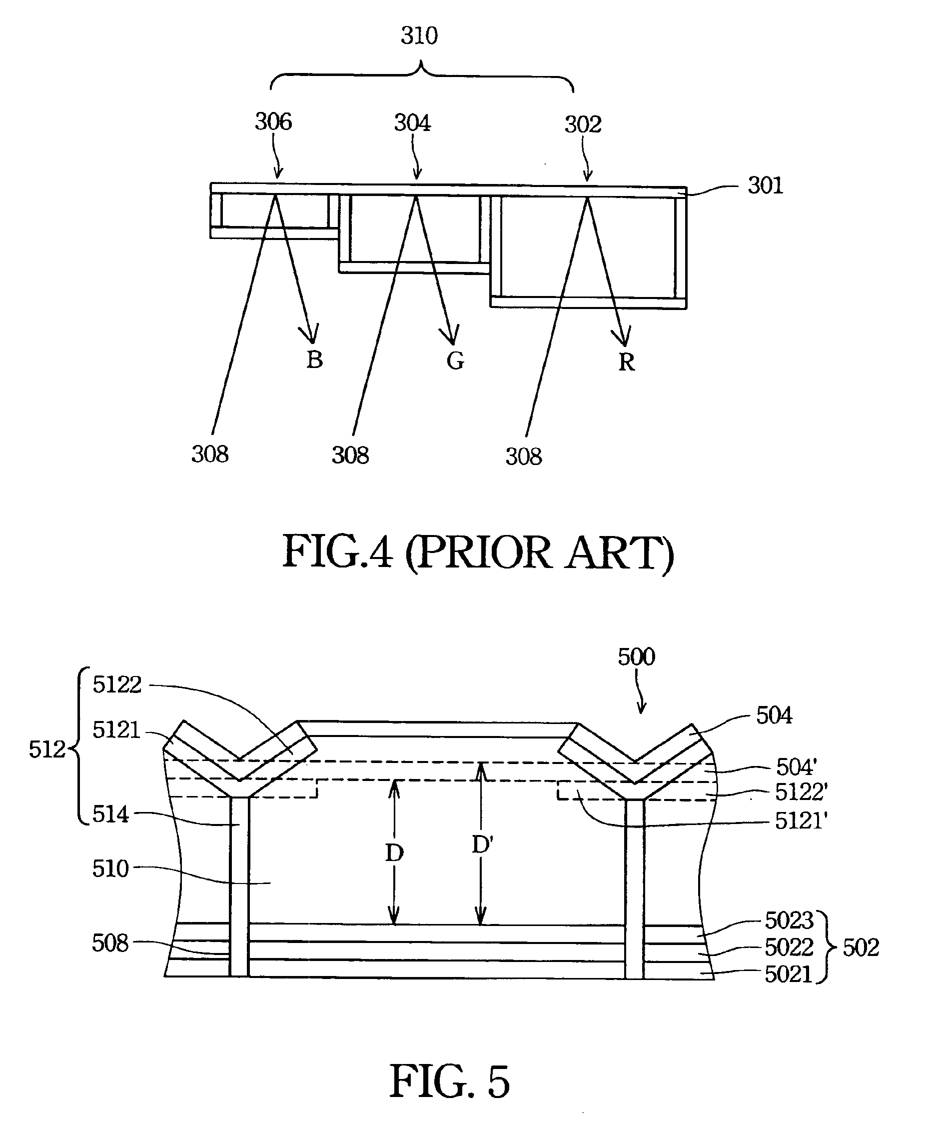
[0027]FIG. 5 depict an optical interference display unit structure according to the first preferred embodiment of this invention. Please refer to FIG. 5, an optical interference display unit 500 which functions as a color changeable pixel comprises at least a first plate 502 and a second plate 504. The two plates are set in parallel. The first plate 502 and the second plate 504 are selected from the group consisting of narrowband mirrors, broadband mirrors, non-metal mirrors, metal mirrors and the combination thereof.

[0028]The first plate 502 is a semi-transparent electrode which comprises a conductive substrate 5021, an absorption layer 5022, and a dielectric layer 5023. An incident light going through light incidence electrode 502 is partially absorbed by the absorption layer 5022. The conductive substrate 5021 is made from a conductive transparent material, such as ITO and IZO. The absorption layer 5022 is made from metal, such as aluminum or silver. The dielectric layer 5023 is ...

embodiment 2

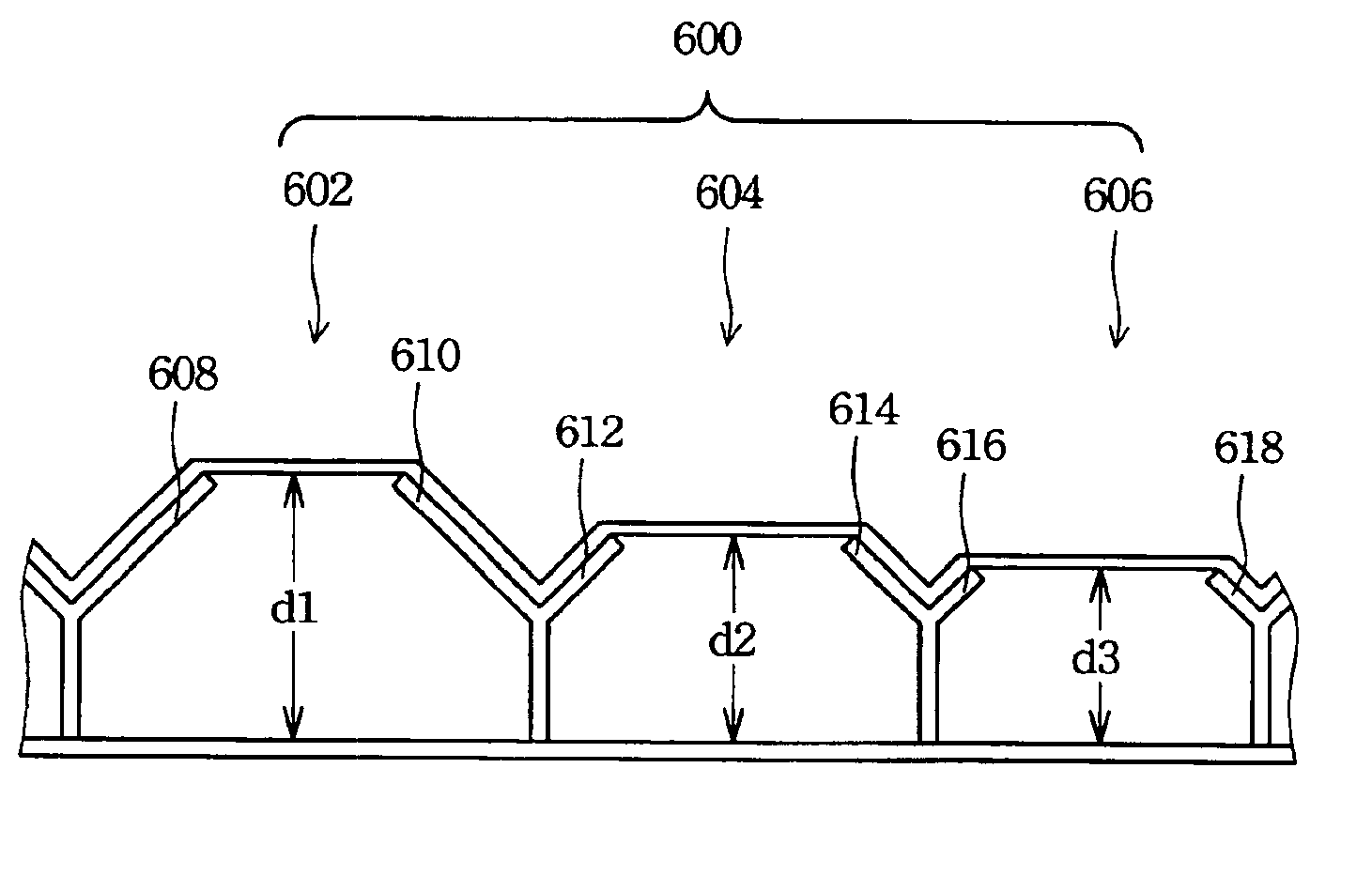
[0032]Referring is made to FIG. 6, FIG. 6 shows a cross-section view of an array of the optical interference display unit provided in the second embodiment of this invention. An array of modulation 600 comprises three optical interference display units: optical interference display unit 602, optical interference display unit 604 and optical interference display unit 606. Every optical interference display unit is a color changeable pixel. The structure of optical interference display unit is the same as the one provided in embodiment 1. The difference of the three optical interference display units is the arms of the posts of the optical interference display unit. The optical interference display unit 602 is supported by arms 608 and 610, the optical interference display unit 604 is supported by arms 612 and 614, and the optical interference display unit 606 is supported by arms 616 and 618. The length and the thickness of the arms 608 and 610, arms 612 and 614, and arms 616 and 618...


PUM

PropertyMeasurementUnit
lengthaaaaaaaaaa
thicknessaaaaaaaaaa
transparent conductiveaaaaaaaaaa

Abstract

A structure of an interference display cell is provided. The cell comprises a first plate and a second plate, wherein a support is located between the first plate and the second plate. The second plate is a deformable and reflective plate. An incident light from one side of the first plate is modulated and only specific frequency light reflects by the second plate. The frequency of the reflected light is related to the distance between the first plate and the second plate. The support has at least one arm. The arm's stress makes the arm hiking upward or downward. The distance between the first plate and the second plate is also changed. Therefore, the frequency of the reflected light is altered.

Description

FIELD OF THE INVENTION[0001]The present invention relates to a structure of an optical interference display. More particularly, the present invention relates to a structure of an optical interference display with posts of arms.BACKGROUND OF THE INVENTION[0002]Planar displays are popular for portable displays and displays with space limits because they are light and small in size. To date, planar displays in addition to liquid crystal displays (LCD), organic electro-luminescent displays (OLED), plasma display panels (PDP) and so on, as well as a mode of the optical interference display are of interest.[0003]U.S. Pat. No. 5,835,255 discloses an array of display units of visible light that can be used in a planar display. Please refer to FIG. 1, which depicts a cross-sectional view of a display unit in the prior art. Every optical interference display unit 100 comprises two walls, 102 and 104. Posts 106 support these two walls 102 and 104, and a cavity 108 is subsequently formed. The d...

Claims


Application Information

Patent Timeline
Patent Type & Authority Patents(United States)
IPC IPC(8): G02B5/28G02B5/20G02F1/1335G02B26/00G02F1/19
CPCB81C1/00182G02B26/001G02B5/284G02B5/201B81B2201/047A01K91/053
Inventor LIN, WEN-JIANTSAI, HSIUNG-KUANG
Owner SNAPTRACK
Why Eureka
Try Eureka