White OLED having multiple white electroluminescence units
Active Publication Date: 2006-02-23
GLOBAL OLED TECH
View PDF9 Cites 235 Cited by
Summary
Abstract
Description
Claims
Application Information
AI Technical Summary
This helps you quickly interpret patents by identifying the three key elements:
Problems solved by technology
Method used
Benefits of technology
Benefits of technology
[0018] An advantage of the present invention is that the white OLED device made with the tandem structure can have high luminous efficiency and high brightness. As a result, the device has longer lifetime when driving it under lower current density while keeping the same required brightness.
[0019] Another advantage of the present invention is that color stability is improved.
[0020] Yet another advantage of the present invention is that device fabrication is simplified.
Problems solved by technology
However, an OLED device will rapidly degrade when driven at high current density.
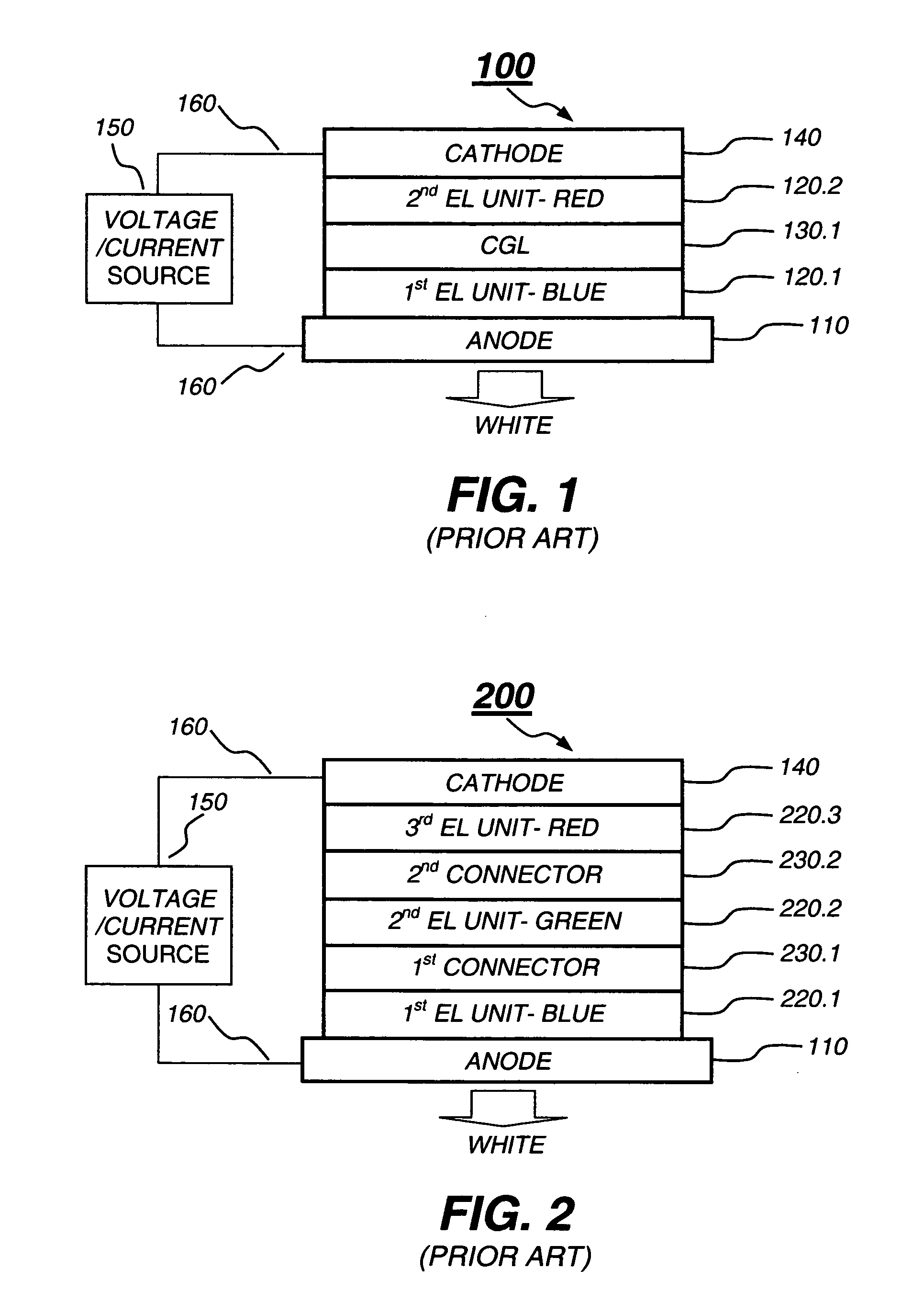
However, the prior art has only taught how to construct a tandem white OLED device using multiple EL units, each unit having a different primary color emission, i.e., having a red, green, or a blue color emission from each of the EL units.
Moreover, device fabrication will be more complicated and more time consuming because each EL unit has a different layer structure.
Method used
Image
Click on the blue label to locate the original text in one second.
Reading with bidirectional positioning of images and text.
Examples
example 2
[0142] A tandem white OLED was constructed in the manner described in Example 1, and the deposited layer structure is:
1. 1st EL Unit:
[0143] The 1st EL unit is the same as the EL unit in Example 1.
2. 1st Intermediate Connector:
[0144] a) an n-type doped organic layer, 30 nm thick, including Alq doped with about 1.2 vol. % lithium; and [0145] b) a p-type doped organic layer, 30 nm thick, including NPB doped with about 4 vol. % “2,3,5,6-tetrafluoro-7,7,8,8-tetracyanoquinodimethane” (F4-TCNQ).
3. 2nd EL Unit:
[0146] The 2nd EL unit is the same as the EL unit in Example 1 except that the thickness of the NPB layer (HTL) is changed from 90 nm to 20 nm.
4. Cathode: approximately 210 nm thick, including Mg:Ag.
[0147] When tested at 20 mA / cm2, this tandem white OLED device has a luminance of 2712 cd / m2 and a luminous efficiency of about 13.6 cd / A. The CIEx and CIEy are 0.325, 0.344, respectively. The EL spectrum is shown in FIG. 17 and the luminous efficiency characteristics are shown...
example 4
[0156] A tandem white OLED was constructed in the manner described in Example 1, and the deposited layer structure is:
1. 1st EL Unit:
[0157] a) an HTL, about 30 nm thick, including NPB; [0158] b) a first LEL, 30 nm thick, including NPB doped with about 2 vol. % “2,8-di-tert-butyl-5,11-di(p-tert-butylphenyl)-6,12-di([1,1′-biphenyl]-4-yl)naphthacene” (yellow emitting layer); [0159] c) a second LEL, 40 nm thick, including 70 vol. % A-DN, 28 vol. % NPB, and about 2 vol. % “4-(di-p-tolylamino)-4′-[(di-p-tolylamino)styryl]stilbene” (blue emitting layer); and [0160] d) an ETL, 10 nm thick, including Bphen.
2. 1st Intermediate Connector: [0161] a) an n-type doped organic layer, 10 nm thick, including Bphen doped with about 1.2 vol. % lithium; and [0162] b) a metal compound layer, 2 nm thick, including WO3.
3. 2nd EL Unit: [0163] a) an HTL, about 70 nm thick, including NPB; [0164] b) a first LEL, 30 nm thick, including NPB doped with about 2 vol. % “2,8-di-tert-butyl-5,11-di(p-tert-butyl...
PUM
Property
Measurement
Unit
Thickness
aaaaa
aaaaa
Thickness
aaaaa
aaaaa
Thickness
aaaaa
aaaaa
Abstract
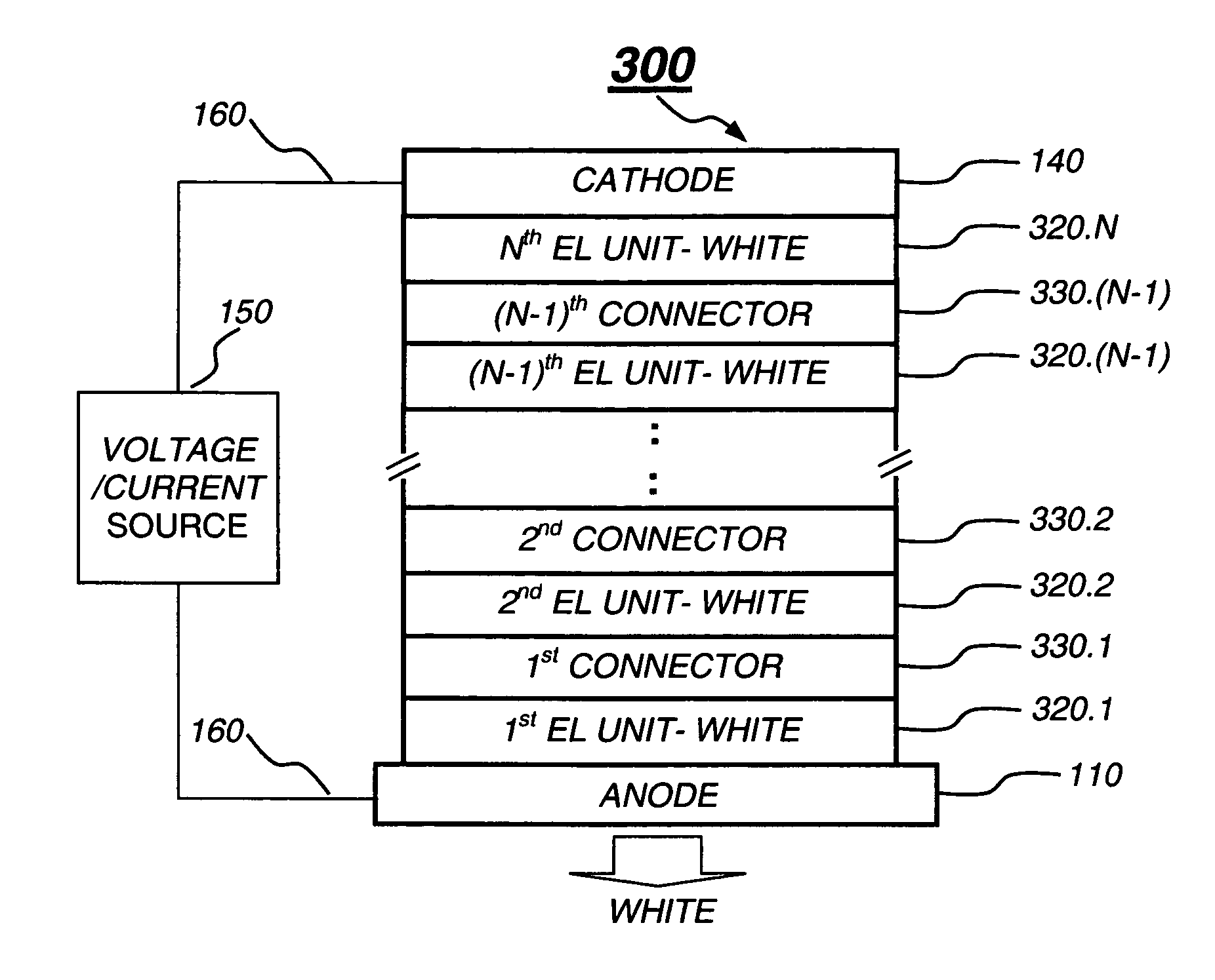
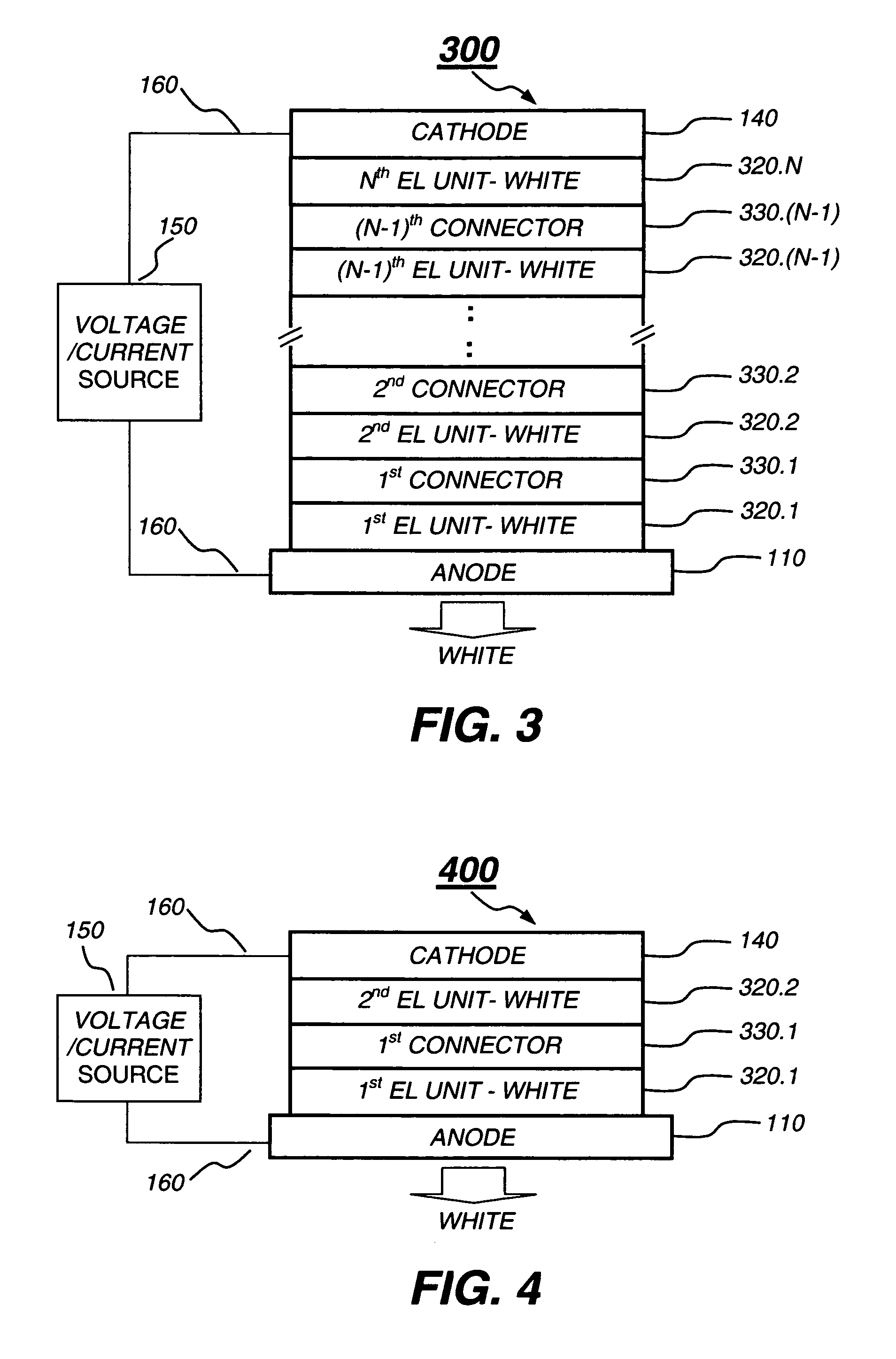
A tandem white OLED device includes an anode, a cathode, and a plurality of organic electroluminescence units disposed between the anode and the cathode, wherein each organic electroluminescence unit includes at least one light-emitting layer, and wherein each organic electroluminescence unit emits white light. The device also includes an intermediate connector disposed between each adjacent organic electroluminescence unit, wherein the intermediate connector includes at least two different layers, and wherein the intermediate connector has no direct connection to an external power source.
Description
CROSS REFERENCE TO RELATED APPLICATIONS [0001] Reference is made to commonly assigned U.S. patent application Ser. No. 10 / 437,195 filed May 13, 2003 by Liao et al., entitled “Cascaded Organic Electroluminescent Device Having Connecting Units with n-Type and p-Type Organic Layers”; U.S. patent application Ser. No. 10 / 857,516 filed May 28, 2004 by Liang-Sheng Liao et al., entitled “Tandem OLED Having Stable Intermediate Connectors”; and U.S. patent application Ser. No. 10 / 882,834 filed Jul. 1, 2004 by Tukaram K. Hatwar et al., entitled “High Performance White Light-Emitting OLED Device”, the disclosures of which are herein incorporated by reference.FIELD OF INVENTION [0002] The present invention relates to providing a plurality of white organic electroluminescence (EL) units to form a tandem white organic electroluminescent device. BACKGROUND OF THE INVENTION [0003] An organic light-emitting diode device, also called an OLED device, commonly includes a substrate, an anode, a hole-tran...
Claims
Application Information
Patent Timeline
Application Date:The date an application was filed.
Publication Date:The date a patent or application was officially published.
First Publication Date:The earliest publication date of a patent with the same application number.
Issue Date:Publication date of the patent grant document.
PCT Entry Date:The Entry date of PCT National Phase.
Estimated Expiry Date:The statutory expiry date of a patent right according to the Patent Law, and it is the longest term of protection that the patent right can achieve without the termination of the patent right due to other reasons(Term extension factor has been taken into account ).
Invalid Date:Actual expiry date is based on effective date or publication date of legal transaction data of invalid patent.

