Interference display unit

a technology of interference display and display unit, which is applied in the direction of optical elements, instruments, coatings, etc., can solve the problems of high cost of complicated manufacturing process and inability to increase yield, and achieve the effect of high brightness

Inactive Publication Date: 2006-02-07
SNAPTRACK
View PDF5 Cites 235 Cited by
  • Summary
  • Abstract
  • Description
  • Claims
  • Application Information

AI Technical Summary

Benefits of technology

[0018]It is therefore an objective of the present invention to provide a method for manufacturing an optical interference display unit structure, and the method is suitable for manufacturing a color optical interference display with resolution and high brightness.
[0019]It is another an objective of the present invention to provide a method for manufacturing an optical interference display unit structure, and the method is suitable for manufacturing a color optical interference display with a simple and easy manufacturing process and high yield.
[0024]Additionally, the arms of the post with the ratios of various length to thickness have various amounts of stress, and displacements and directions generated by arms are various during baking. Therefore, the arms with the ratios of various lengths to thickness and the thickness of the second wall may be used for controlling the length of the cavity, instead of the various thickness of the sacrificial layers used in the various processes of the display units to control various wavelengths of light reflected in the prior art. There are many advantages in the above way. First of all, the cost drops drastically. The thickness of the cavity in the prior art is the thickness of the sacrificial layer, and the sacrificial layer needs to be removed at the end of the process. However, using an upward displacement of the second wall in the present invention increases the length of the cavity, so that the length of the cavity is greater than the thickness of the sacrificial layer, even if the thickness of the sacrificial layer is substantially decreased while forming the same length of cavities. Therefore, the material used for manufacturing the sacrificial layer is substantially reduced. The second, the process time is shortened. The release etching process of the metal sacrificial layer in the prior art consumes lots of time, because the sacrificial layer is removed by an etching gas that must permeate the spaces between the posts. The present invention utilizes a mask for a front exposure, so the sacrificial layer can be transparent materials such as dielectric materials, instead of opaque materials such as metal and the like as in the prior art. Besides, the thickness used by the sacrificial layer can be substantially reduced, so the time required for the release etching process can be also drastically decreased. Third, the color optical interference display formed by using posts can substantially reduce complexity of the process. The difference in the ratios of thickness of the second wall is used for changing the stress of the second wall. After baking, various optical interference display units have various lengths of the cavities due to the displacement of the second wall, such that reflected light is changed with various wavelengths, such as red, green, and blue lights, so as to obtain various color lights.
[0028]In accordance with the color planar display consisting of an array of optical interference display units disclosed by the present invention, the advantages of a matrix color planar display according to the prior art are retained, including high resolution and high brightness, as well as the advantages of a multi-layered color planar display with a simple process and high yield in the prior art. It is understood that the present invention discloses an optical interference display unit which not only keeps all advantages of the prior optical interference color planar display such as high resolution, high brightness, simple process and high yield during forming arrays, but also increases the window during processing and raises the yield of the optical interference color planar display.

Problems solved by technology

The cost of the complicated manufacturing process is higher, and the yield cannot be increased due to the complicated manufacturing process.

Method used


Image

  • Interference display unit
  • Interference display unit
  • Interference display unit

Examples


embodiment 1

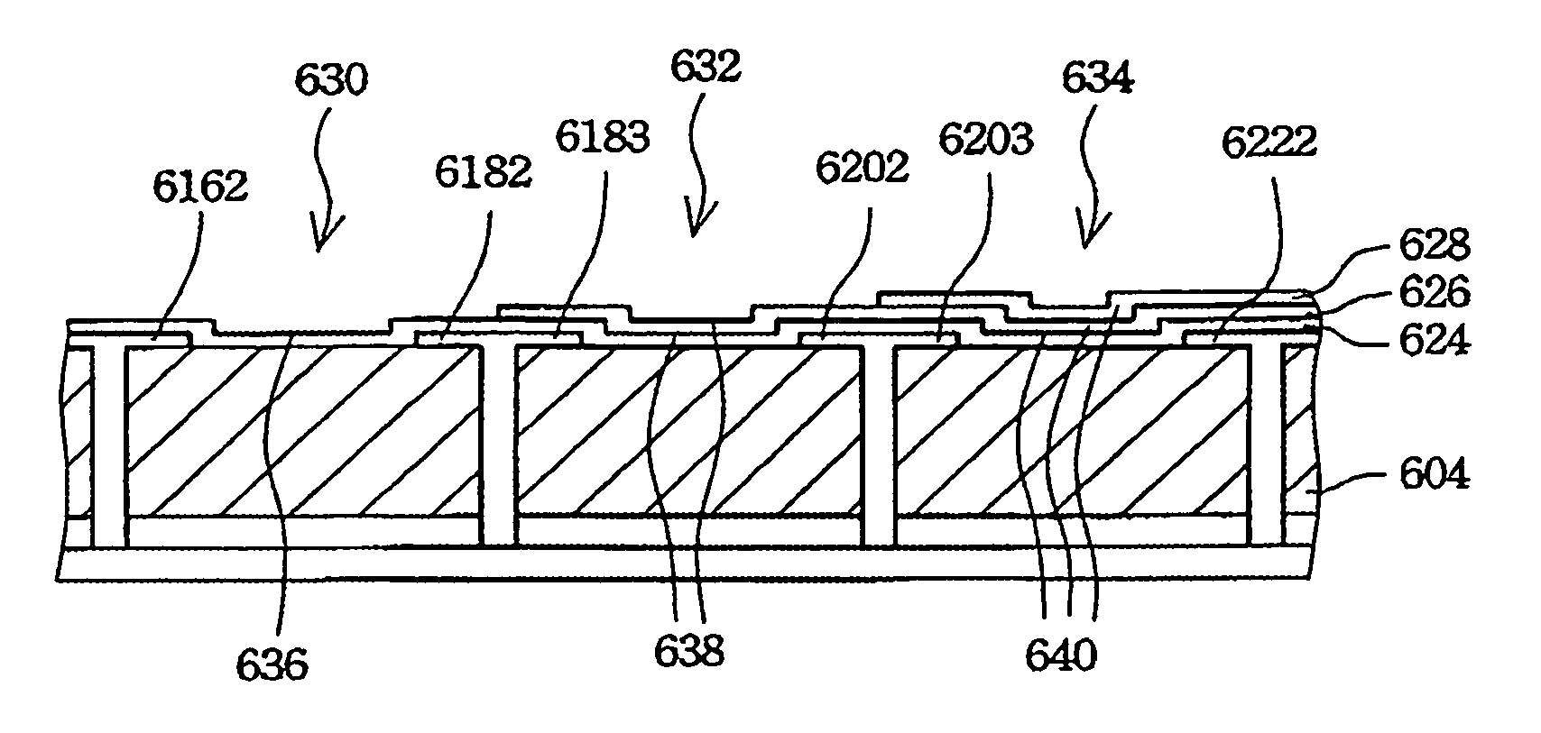
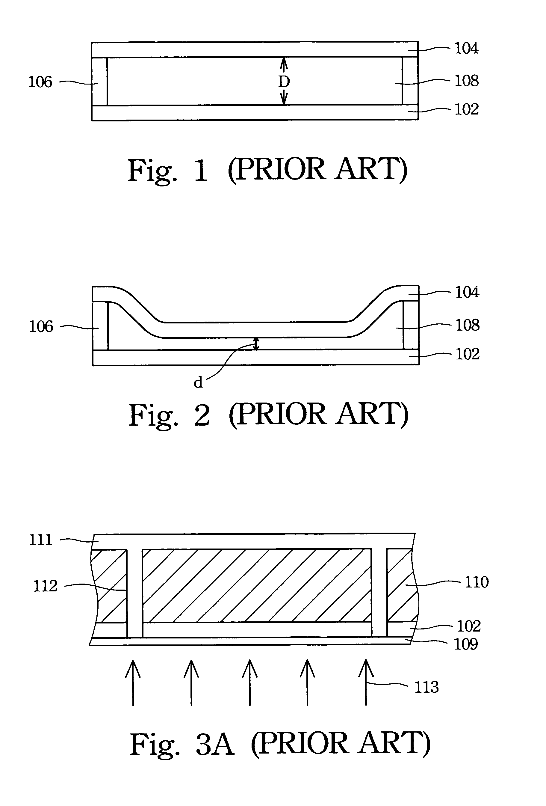
[0038]FIGS. 6A to 6E depict a method for manufacturing an optical interference display unit according to a preferred embodiment of the invention. Please referring to FIG. 6A first, a first electrode 602 and a sacrificial layer 604 are formed in order on a transparent substrate 601. The sacrificial layer 604 is made of transparent materials such as dielectric materials, or opaque materials such as metal materials. Opening 606, 608, 610 and 612 are formed in the first electrode 602 and the sacrificial layer 604 by a photolithographic etching process. The openings 606, 608, 610 and 612 are suitable for forming a post therein.

[0039]Next, a material layer 614 is formed on the sacrificial layer 604 and fills the openings 606, 608, 610 and 612. Openings 606 and 608, openings 608 and 610, and openings 610 and 612 are used to define the location of the optical interference display units 630, 632 and 634. The material layer 614 is suitable for forming posts, and the material layer 614 general...


PUM

PropertyMeasurementUnit
thicknessaaaaaaaaaa
lengthaaaaaaaaaa
stressaaaaaaaaaa

Abstract

An interference display unit with a first electrode, a second electrode and posts located between the two electrodes is provided. The characteristic of the interference display unit is that the second electrode's stress is released through a thermal process. The position of the second electrode is shifted and the distance between the first electrode and the second electrode is therefore defined. A method for fabricating the structure described as follow. A first electrode and a sacrificial layer are sequentially formed on a substrate and at least two openings are formed in the first electrode and the sacrificial layer. A supporter is formed in the opening and the supporter may have at least one arm on the top portion of the supporter. A second electrode is formed on the sacrificial layer and the supporter and a thermal process is performed. Finally, The sacrificial layer is removed.

Description

FIELD OF INVENTION[0001]The present invention relates to a method for manufacturing an optical interference display. More particularly, the present invention relates to a method for manufacturing an optical interference display with posts of arms.BACKGROUND OF THE INVENTION[0002]Planar displays are popular for portable displays and displays with space limits because they are light and small in size. To date, planar displays in addition to liquid crystal displays (LCD), organic electro-luminescent displays (OLED), plasma display panels (PDP) and so on, as well as a mode of the optical interference display are of interest.[0003]U.S. Pat. No. 5,835,255 discloses an array of display units of visible light that can be used in a planar display. Please refer to FIG. 1, which depicts a cross-sectional view of a display unit in the prior art. Every optical interference display unit 100 comprises two walls, 102 and 104. Posts 106 support these two walls 102 and 104, and a cavity 108 is subseq...

Claims


Application Information

Patent Timeline
Patent Type & Authority Patents(United States)
IPC IPC(8): G02F1/03G02F1/07G02F1/1343B81B3/00B81C1/00G02B5/20G02B5/28G02B26/00
CPCB81C1/00182G02B26/001G02B5/284G02B5/201B81B2201/047G02F1/1343
Inventor LIN, WEN-JIAN
Owner SNAPTRACK
Why Eureka
Try Eureka