Liquid crystal display device

a display device and liquid crystal technology, applied in static indicating devices, instruments, non-linear optics, etc., can solve the problems of image quality degradation, insufficient viewing angle characteristics, and insufficient holding rate, and achieve excellent contrast, wide viewing angle display, and higher display quality

Inactive Publication Date: 2009-01-01
SEMICON ENERGY LAB CO LTD
View PDF6 Cites 146 Cited by
  • Summary
  • Abstract
  • Description
  • Claims
  • Application Information

AI Technical Summary

Benefits of technology

[0087]By the present invention, a wide viewing angle display can be realized. Alternatively, a display device which has excellent in contrast can be obtained. Alternatively, a display device higher display quality can be obtained. Alternatively, a display device which is less likely to be influenced by noise and can perform clear display can be provided. Alternatively, a display device in which display degradation is less likely to be caused can be provided. Alternatively, a display device which has the long life time can be provided.

Problems solved by technology

However, the viewing angle characteristics are not enough, and further improvement is required as a display device.
Although liquid crystal has a voltage holding property, the holding rate is not 100%, and there is concern about a leak by charge passing to liquid crystal.
As a result, desired gray scale can not be obtained, or the image quality is degraded.
Thus, the display quality is gradually degraded in course of time, so that the life of products is shortened.
Specifically, a display device of a normally black mode can not display black color, which leads to low contrast.

Method used


Image

  • Liquid crystal display device
  • Liquid crystal display device
  • Liquid crystal display device

Examples


embodiment mode 1

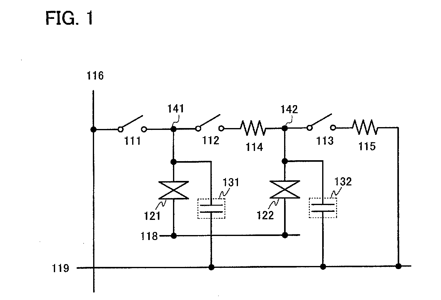
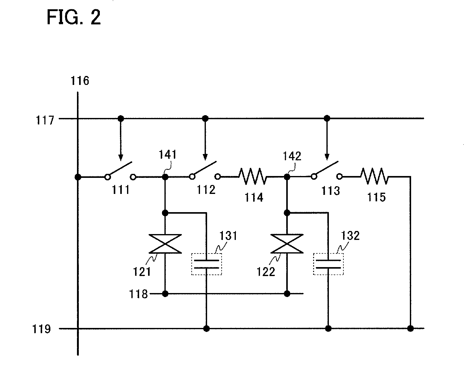
[0167]A basic configuration of a pixel of the present invention is described with reference to FIG. 1. A pixel shown in FIG. 1 includes a first switch 111, a second switch 112, a third switch 113, a first resistor 114, a second resistor 115, a first liquid crystal element 121, a second liquid crystal element 122, a first storage capacitor 131, and a second storage capacitor 132. In addition, the pixel is connected to a signal line 116 and a Cs line 119. Note that each of the first liquid crystal element 121 and the second liquid crystal element 122 includes a pixel electrode, a common electrode 118, and liquid crystal controlled by the pixel electrode and the common electrode 118.

[0168]In FIG. 1, the pixel electrode of the first liquid crystal element 121 is connected to the signal line 116 through the first switch 111. In addition, the pixel electrode of the first liquid crystal element 121 is connected to the pixel electrode of the second liquid crystal element 122 through the sec...

embodiment mode 2

[0217]In this embodiment mode, a structure which is different from that of Embodiment Mode 1 is described with reference to FIG. 18. In Embodiment Mode 1, although the potentials which are applied to the pixel electrodes of the first liquid crystal element and the second liquid crystal element are determined by resistance division between the signal line and the Cs line, the Cs line is not necessarily used. This embodiment mode will show one example of that.

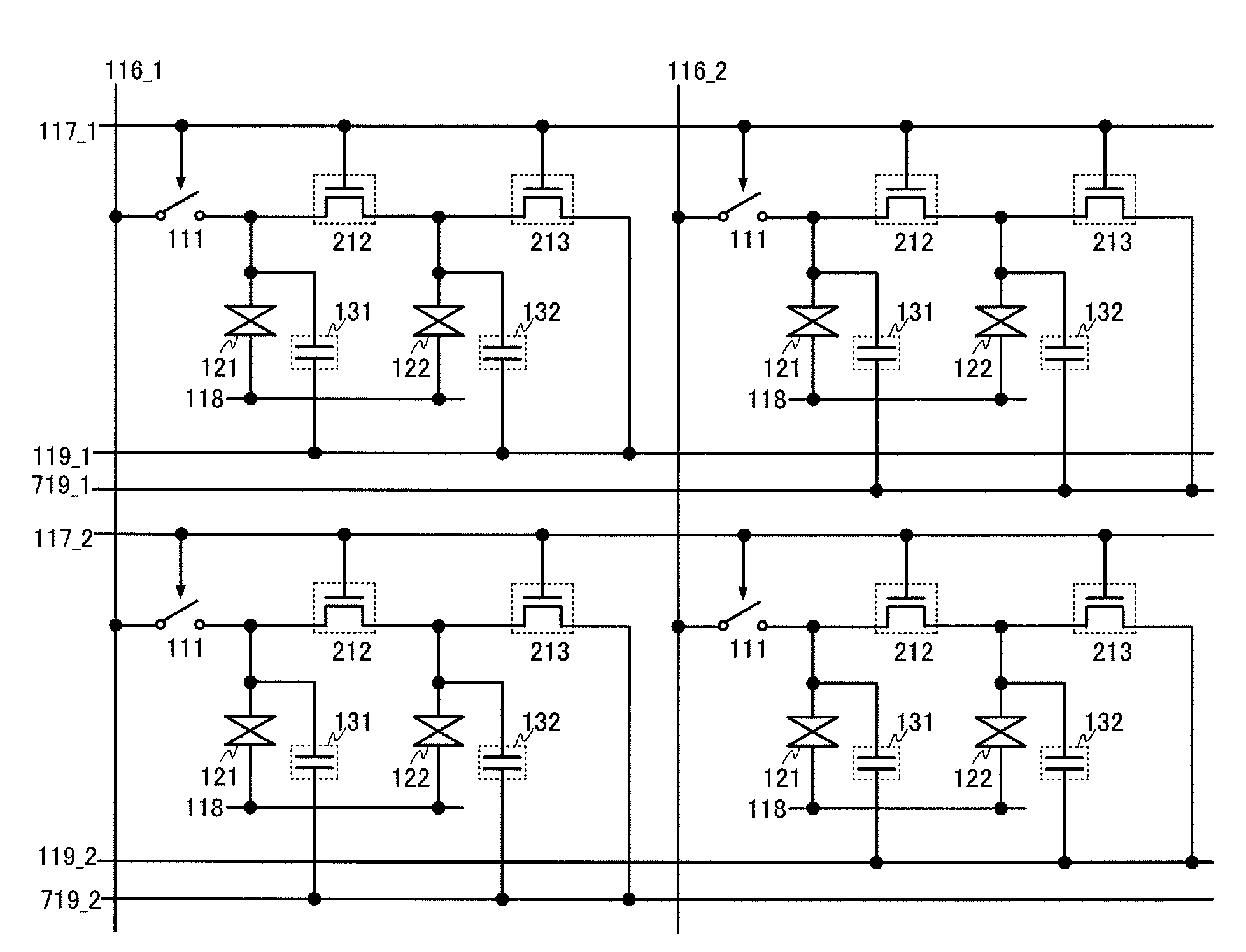
[0218]A pixel 1200 shown in FIG. 18 includes the switch 111, the transistor 212, the transistor 213, the first liquid crystal element 121, the second liquid crystal element 122, the first storage capacitor 131, and the second storage capacitor 132. Note that the pixel 1200 is connected to the signal line 116, the scan line 117, the Cs line 119, and a potential supply line 1219. In other words, the pixel 1200 has a structure in which one electrode of the transistor 213 is connected to not to the Cs line 119 but the potential suppl...

embodiment mode 3

[0230]In this embodiment mode, an example of the pixel structure which is different from those of Embodiment Modes 1 and 2 is described. A pixel shown in FIG. 22 includes the switch 111, the transistor 212, the transistor 213, the first liquid crystal element 121, the second liquid crystal element 122, the first storage capacitor 131, the second storage capacitor 132, and a third storage capacitor 1601. Note that the pixel shown in FIG. 22 is connected to the signal line 116, the scan line 117, and the Cs line 119, and has a structure where the third storage capacitor 1601 is provided between the node 142 and one electrode of the transistor 213 in the pixel shown in FIG. 4 in Embodiment Mode 1. Reference numerals denoting the same components as those in FIG. 4 are used in common throughout the drawings, and the description is omitted.

[0231]The pixel shown in FIG. 22 can be operated in a similar manner to the pixel shown in FIG. 4. Note that by providing the third storage capacitor 1...


PUM

PropertyMeasurementUnit
resistanceaaaaaaaaaa
widthaaaaaaaaaa
channel lengthaaaaaaaaaa

Abstract

The present invention has a pixel which includes a first switch, a second switch, a third switch, a first resistor, a second resistor, a first liquid crystal element, and a second liquid crystal element. A pixel electrode of the first liquid crystal element is electrically connected to a signal line through the first switch. The pixel electrode of the first liquid crystal element is electrically connected to a pixel electrode of the second liquid crystal element through the second switch and the first resistor. The pixel electrode of the second liquid crystal element is electrically connected to a Cs line through the third switch and the second resistor. A common electrode of the first liquid crystal element is electrically connected to a common electrode of the second liquid crystal element.

Description

BACKGROUND OF THE INVENTION[0001]1. Field of the Invention[0002]The present invention relates to an object, a method, or a method to produce an object. The present invention particularly relates to a display device or a semiconductor device, and further relates to an electronic device including the display device in a display portion.[0003]2. Description of the Related Art[0004]Liquid crystal display devices are used for many kinds of electronic devices such as a mobile telephone, a television receiver, and the like, and many researches are done for further improving the quality.[0005]While advantages of a liquid crystal display device are small size, light weight, and low power consumption compared to a CRT (cathode-ray tube) and, a problem of the liquid crystal display device is the narrow viewing angle. In recent years, many researches about a multi domain method, that is, an alignment division method are made for improving viewing angle characteristics. For example, an MVA (mult...

Claims


Application Information

Patent Timeline
Patent Type & Authority Applications(United States)
IPC IPC(8): G02F1/136
CPCG09G3/342G09G3/3655G09G3/3659G09G3/3688G09G2300/0426G09G2300/0443G09G2300/0842G09G2300/0852G09G2310/024G09G2310/0251G09G2310/0297G09G2320/0238G09G2320/0252G09G2320/0257G09G2320/0261G09G2320/028G09G2340/02G09G2340/0435G09G2340/16G02F1/136213G02F1/13624G02F1/136286G02F1/1368G02F2201/121G02F2201/123G02F2202/10G02F1/133621
Inventor KIMURA, HAJIME
Owner SEMICON ENERGY LAB CO LTD
Why Eureka
Try Eureka