Encapsulated component which is small in terms of height and method for producing the same

a technology of encapsulated components and components, which is applied in the direction of electrical apparatus casings/cabinets/drawers, hermetically sealed casings, coupling device connections, etc., can solve the problems of moisture penetration into the component structure and problematic encapsulation, and achieve good contrast, dissipate pyrovoltages, and improve bonding

Inactive Publication Date: 2006-01-03
SNAPTRACK
View PDF14 Cites 54 Cited by
  • Summary
  • Abstract
  • Description
  • Claims
  • Application Information

AI Technical Summary

Benefits of technology

[0008]In contrast to known encapsulated components, the inventive component has the advantage of a lower overall height because the distance between chip and carrier substrate is minimized, since the surface of the chip already lies on the carrier substrate.
[0035]A metallization applied to the back side of the chip can serve in an inventive manner for production of an inscription of the component. For this, via this metallization a lacquer layer is applied that forms a color contrast with the metallization. Via laser writing, the lacquer layer is selectively removed and the writing effect is achieved. To produce a contrast effect, other auxiliary layers that can be lifted with lasers can also be generated over the metallization. For example, different metallization layers are also suitable insofar as they can form a contrary optical contrast. This contrast can also exist in different reflection effects of the metallization, or in a different metal color. For example, black nickel is particularly suitable as a contrast agent. This forms a good contrast with metallic reflective metallizations or with copper.

Problems solved by technology

However, such an encapsulation is problematic for components that bear component structures on a surface that are sensitive to a direct embedding.
However, what is disadvantageous in this method is the elaborate lamination process for application of the foil as well as the wet-chemical or, respectively, galvanic metallization that can, given slight leakages of the foil covering, already lead to a penetration of moisture into the component structures.

Method used


Image

  • Encapsulated component which is small in terms of height and method for producing the same
  • Encapsulated component which is small in terms of height and method for producing the same
  • Encapsulated component which is small in terms of height and method for producing the same

Examples


Embodiment Construction

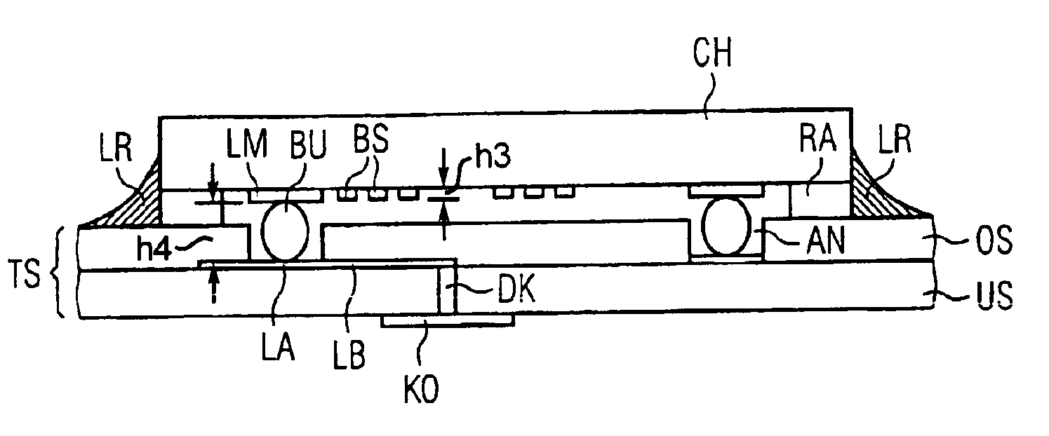
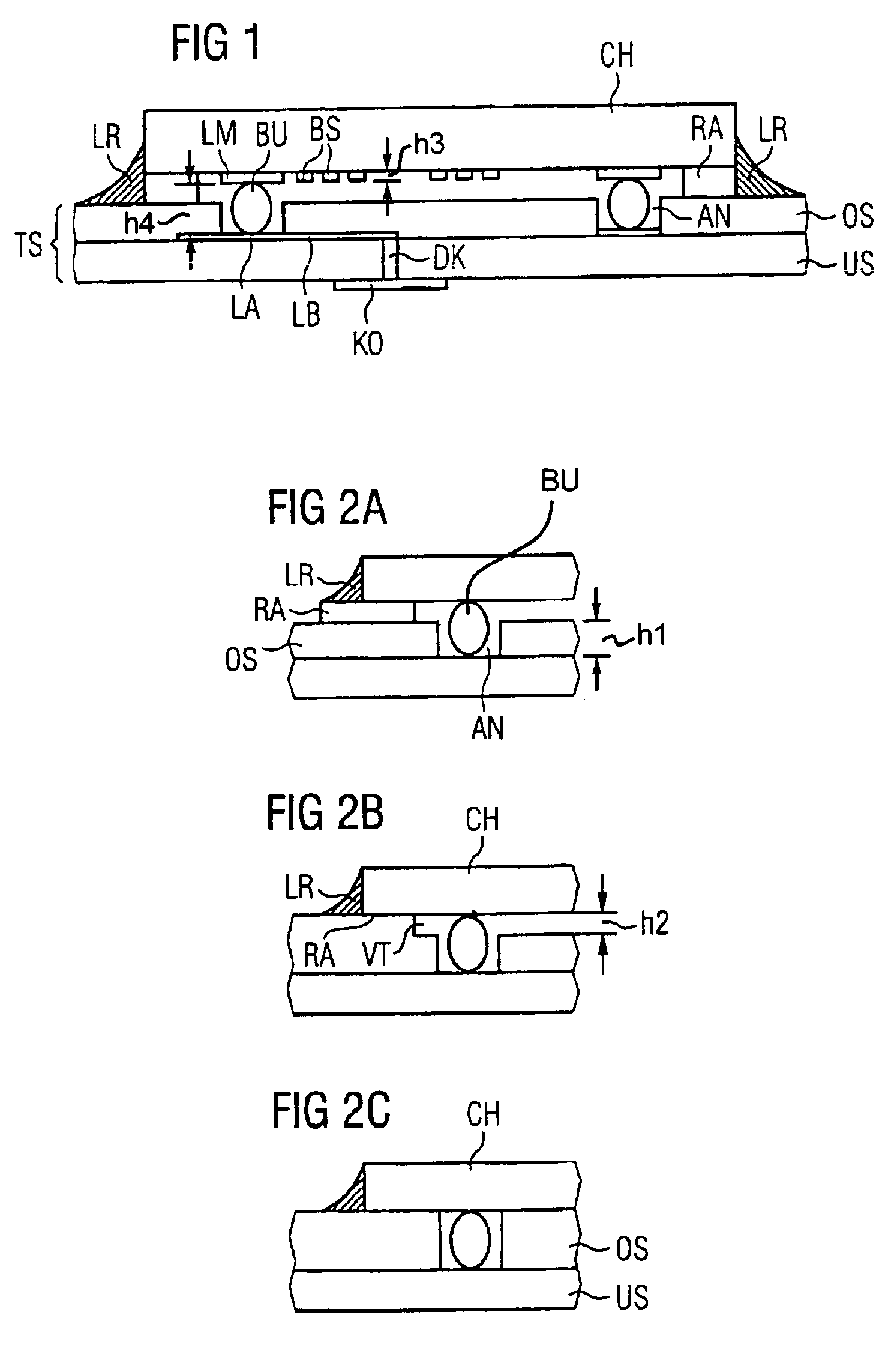
[0048]FIG. 1 shows a first embodiment of an inventive component in schematic cross-section. The component is essentially formed of the chip CH, for example a piezoelectric substrate on whose one surface are applied component structures BS such as, for example, band-shaped metallizations of a surface wave component (SAW component) and which have a height h3. The chip is applied on a carrier substrate TS which comprises at least one upper layer OS and one lower layer US.

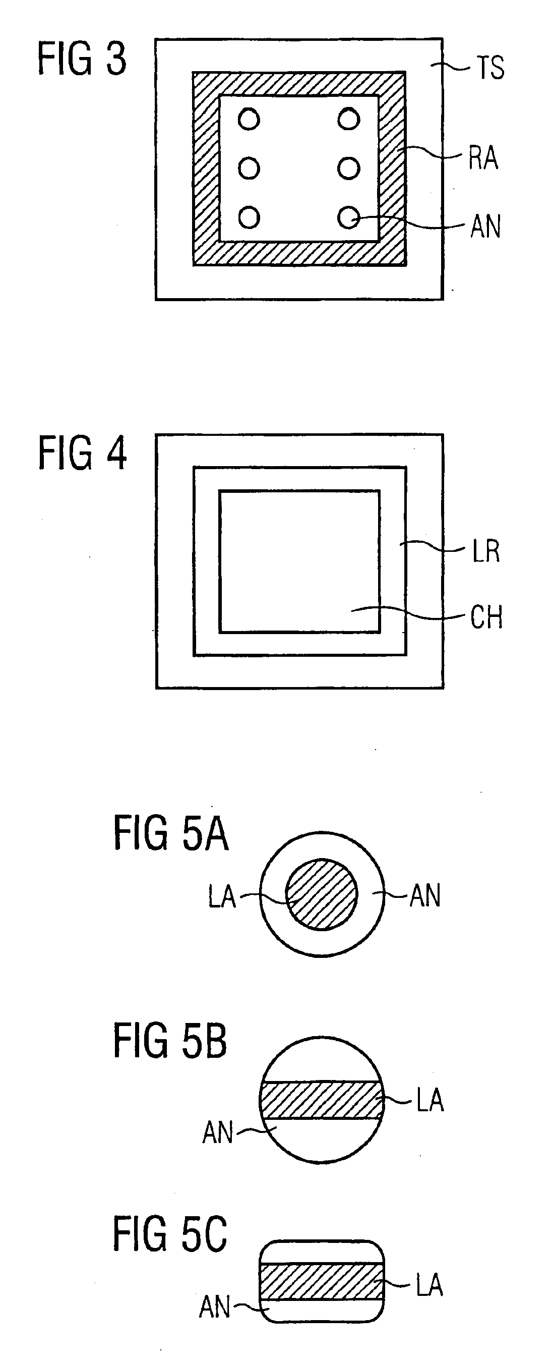
[0049]Recesses AN, which have a depth h1, are provided in the upper layer OS of the carrier substrate TS. On the floor of the recesses, solderable connection areas LA are arranged over which the bump connections BU, which have a height h4, are arranged. The bumps BU connect the solderable connection areas LA with the solderable metallizations LM on the surface of the chip CH. The chip rests on a frame RA which defines the distance between the upper surface of the upper layer OS and the surface of the chip CH and preven...


PUM


Abstract

For simpler and safer encapsulation of components, it is proposed to generate the connection between a chip and a carrier substrate by means of bump connections that are sunk into recesses on the carrier substrate. The component thereby lies directly on the carrier substrate, in particular on a frame circumscribing the component structures on the chip.

Description

BACKGROUND OF THE INVENTION[0001]The invention concerns an encapsulated component with a reduced overall height, in particular a component working with acoustic waves which is constructed on a piezoelectric substrate.[0002]In electrical components, the trend increasingly goes towards components without massive housings. In order to nevertheless protect the components from environmental influences, various methods have already been proposed for simple encapsulation of the components. One possibility is to completely provide a component with a protective layer, for example to completely embed it in plastic, whereby only the electrical connections for the component are free of plastic. However, such an encapsulation is problematic for components that bear component structures on a surface that are sensitive to a direct embedding.[0003]For example, for surface wave components it has already been proposed to cover the component structures arranged on the surface of a piezoelectric substr...

Claims


Application Information

Patent Timeline
Patent Type & Authority Patents(United States)
IPC IPC(8): H01L23/28H05K5/06H01L23/12H01L29/06H03H3/02H03H3/06H03H3/08H03H9/02H03H9/05H03H9/10H03H9/25H03H9/56
CPCH01L24/31H03H9/059H03H9/1078H01L29/0657H01L2224/16225H01L2224/16237H01L2224/73203H01L2224/83951H01L2924/01004H01L2924/01005H01L2924/0101H01L2924/01013H01L2924/0102H01L2924/01029H01L2924/01032H01L2924/01033H01L2924/01046H01L2924/01047H01L2924/01057H01L2924/01078H01L2924/01079H01L2924/01082H01L2924/01088H01L2924/09701H01L2924/10157H01L2924/3025H01L2924/0132H01L2924/01006H01L2924/01068H01L2924/01076H01L2924/0133H01L2224/291H01L2924/1517H01L2924/15787H01L2224/29111H01L2224/83136H01L2224/11334H01L2924/0105H01L2224/13111H01L2924/00014H01L2924/014H01L2924/351H01L2924/12042H01L2224/05573H01L2224/05568H01L2224/0615H01L2924/00
Inventor HOFFMANN, CHRISTIANPORTMANN, JURGENKRUEGER, HANS
Owner SNAPTRACK
Why Eureka
Try Eureka