

Photoimageable dielectric material for circuit protection
a dielectric material and photo-image technology, applied in the field of electro-mechanical circuit devices, can solve the problems of damage, circuit damage, and decrease in electrical performance, and achieve the effect of excellent resistance to corrosive, acidic and/or alkaline environments
- Summary
- Abstract
- Description
- Claims
- Application Information
AI Technical Summary
Benefits of technology
Problems solved by technology
Method used
Image

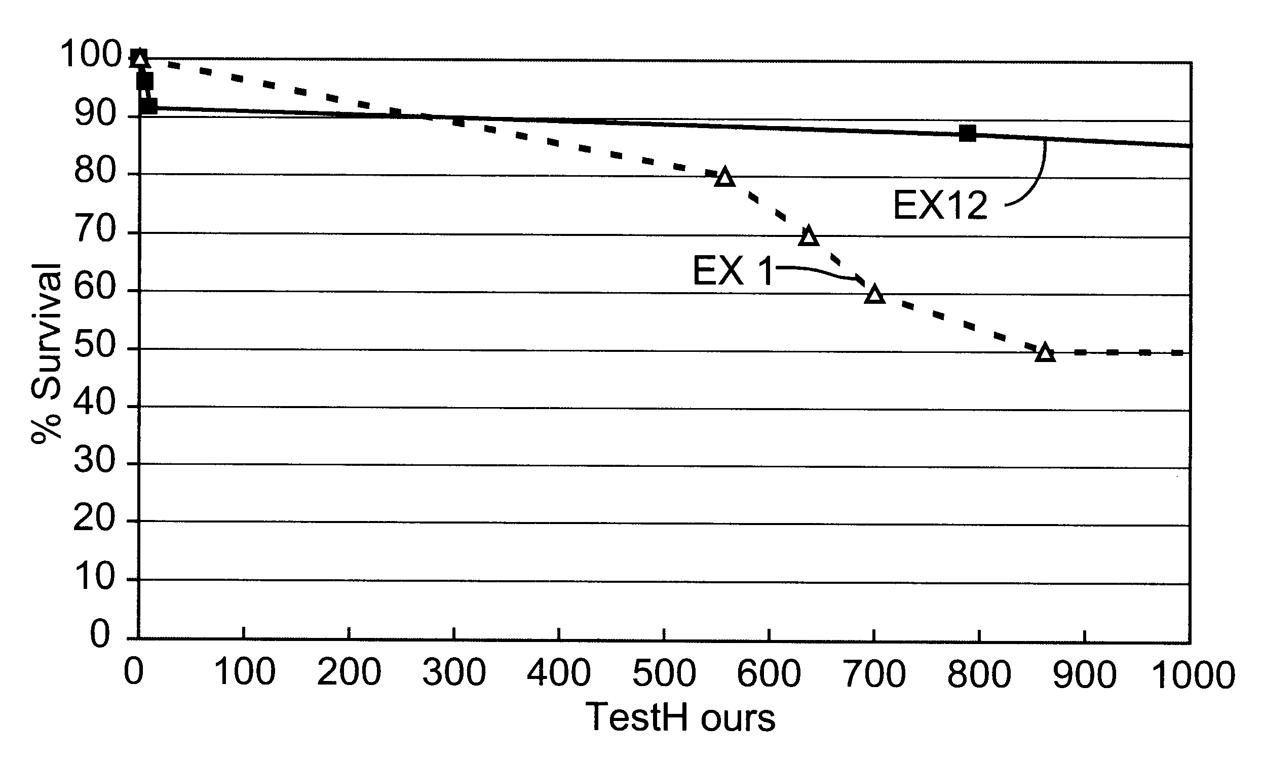
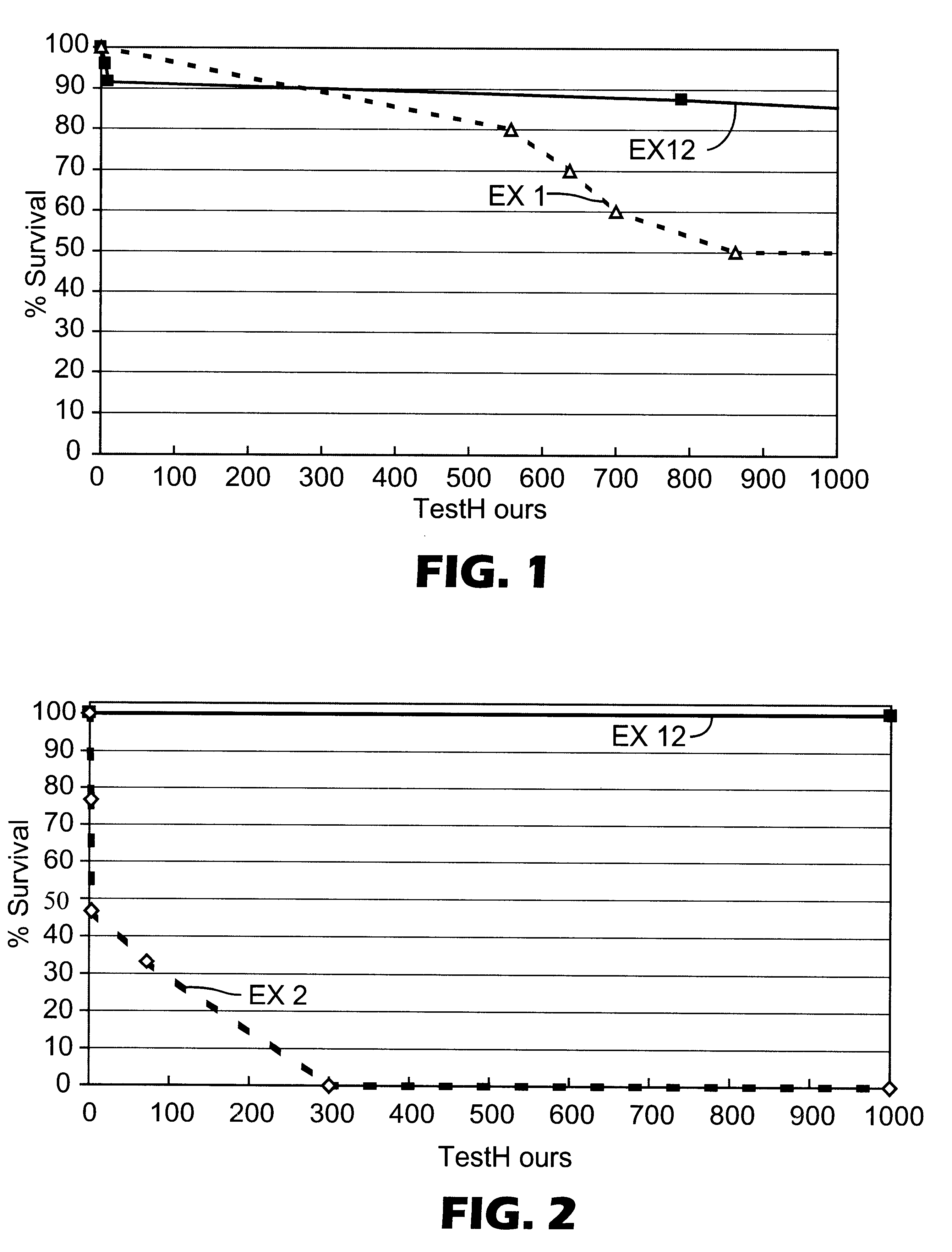
Examples
example 1
This formulation included: Epofriend.RTM. A1020 eSBS Copolymer (97.5%) epoxy modified aromatic vinyl-conjugated diene block copolymer Epon.RTM. 828 epoxy (2.5%): epoxy resin Solid Triarylsulfonium hexafluoroantimonate salt mixture (0.042%): Photoinitiator (PI)
In the following discussion, this will be referenced as the "base formulation". This material was melt compound extruded onto a silicone-treated release liner at a thickness of approximately 70 .mu.m (2.75 mils). The resulting film material was hot roll laminated 82.degree. C. onto a strip of flex circuitry at a line speed of 0.2-0.3 m / min.
A patterned photomask was positioned adjacent to the circuit / film laminate, which was then exposed to a UV light source. The medium pressure mercury UV light source was set to provide an exposure dosage of 1000 mJ / cm.sup.2 to produce the desired pattern. The laminate was subsequently baked for 15 minutes at 125.degree. C. in air. The unexposed material was developed away in a solvent bath. Us...
examples 2-6
Examples 2 through 6 in Table 1 show formulations which contain constant amounts of the Epofriend.RTM. material and the Epon.RTM. 828 epoxy with different photoinitiator levels. The coating solutions were prepared using the aforementioned solvent process using ethyl acetate as a solvent to facilitate the mixing. A shorthand notation was used to reflect the amount of photoinitiator salt relative to the base formulation. A "1.times." designation represented the 0.042% photoinitiator salt concentration relative to the total amount of dissolved solids.
TABLE 1 Solvent Coated Epoxy & Cyracure-Modified Formulas Example 2 3 4 5 6 Epofriend Solution (g) 75.0 75.0 75.0 75.0 75.0 Epon 828 (g) 0.481 0.481 0.481 0.481 0.481 Catalyst Solution (g) 0.016 0.081 0.161 0.808 1.615 Catalyst content compared 1X 5X 10X 50X 100X to Example 1
examples 7-11
Examples 7-11 in Table 2 show formulations that contain solely the Epofriend.RTM. material and different photoinitiator levels. The coating solutions were prepared using the aforementioned solvent process using ethyl acetate as a solvent to facilitate the mixing.
TABLE 2 Solvent coated Cryacure-Only Modified Formulas Example 7 8 9 10 11 Epofriend Solution (g) 75.0 75.0 75.0 75.0 75.0 Catalyst Solution 0.016 0.079 0.158 0.787 1.575 Catalyst content compared 1X 5X 10X 50X 100X to Example 1
These solutions were coated onto a silicone-coated polyester film so that films approximately 76 .mu.m (3 mils) thick were obtained after evaporating the ethyl acetate solvent at 50-60.degree. C. The dried films were hot roll laminated onto circuitry and exposed to 1000 mJ / cm.sup.2 UV radiation as before. The laminate was subsequently baked for 15-30 minutes at 125.degree. C. in air. Developing was conducted in a Schmiedeskamp Probimer.RTM. 450M developer at a speed of 1 m / min. Sumps 1 and 2 were fill...
PUM
 Abstract
Description
Claims
Application Information