
Organic light emitting diode display pixel arrangement structure and display device

A light-emitting diode and pixel arrangement technology, applied in the direction of electric solid-state devices, semiconductor devices, electrical components, etc., can solve the problems of affecting the display effect, unfavorable organic material evaporation, and complicated OLED manufacturing process, so as to improve the PPI value and resolution , Improve image quality and effect, and display the effect of uniform color

Active Publication Date: 2017-11-10
TRULY HUIZHOU SMART DISPLAY
View PDF5 Cites 0 Cited by
  • Summary
  • Abstract
  • Description
  • Claims
  • Application Information

AI Technical Summary

Problems solved by technology

However, the existing RGB pixel arrangement structure is difficult to meet the high-resolution and high-brightness requirements of electronic devices for display screens. In the case of achieving the same resolution; another existing OLED pixel arrangement structure is to share However, the ratio of R / G / B of the pixels formed by this arrangement is 1: 1: 2, which will affect the display effect of the display. It will be more complicated in the OLED manufacturing process, and it is not conducive to the development of organic materials. Evaporation, easy to mix colors

Method used


Image

  • Organic light emitting diode display pixel arrangement structure and display device
  • Organic light emitting diode display pixel arrangement structure and display device
  • Organic light emitting diode display pixel arrangement structure and display device

Examples


no. 1 example

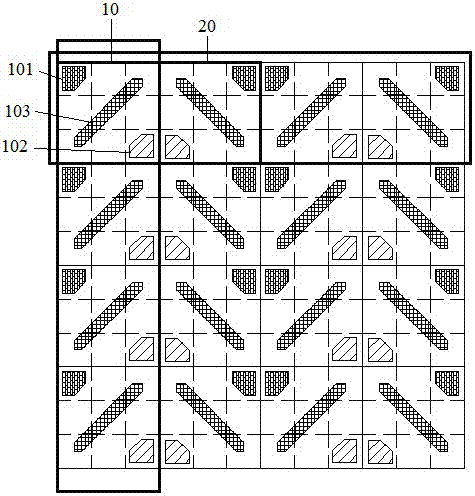
[0031] see Figure 4 , Figure 4 It is a structural schematic diagram of the second embodiment of the pixel arrangement structure of the organic light emitting diode display of the present invention. Compared with the first embodiment, the difference of this embodiment is that: the organic light emitting diode display pixel arrangement structure further includes a third pixel 30 and a fourth pixel 40, wherein the third pixel 30 is opposite to the first pixel 10 The horizontal axis is flipped by 180 degrees, and the fourth pixel 40 is formed by flipping the first pixel 10 of the second pixel 20 by 180 degrees relative to the horizontal axis; in this embodiment, each adjacent first pixel 10, second The pixel 20, the third pixel 30 and the fourth pixel 40 form a basic pixel unit, and the basic pixel unit is closely and repeatedly arranged in the horizontal direction and the vertical direction, wherein the first pixel 10, the second pixel in the basic pixel unit 20. The second s...


PUM


Abstract

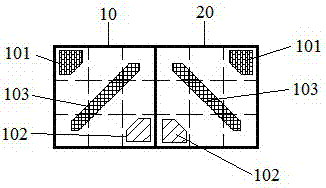
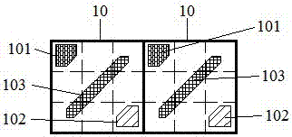
The invention discloses a pixel arrangement structure of an organic light emitting diode display and a display device. The pixel arrangement structure includes a plurality of closely arranged first pixels and / or second pixels, and each first pixel and second pixel has the same size. Each of the first pixel and the second pixel includes a first sub-pixel, a second sub-pixel arranged at two ends of a diagonal of the rectangle, and a third sub-pixel arranged along the other diagonal of the rectangle. The invention improves the aperture ratio of the pixel, makes the arrangement structure of the first sub-pixel, the second sub-pixel and the third sub-pixel more compact, and the display color is more uniform, breaks through the limitations of the FMM manufacturing process and coating process, and effectively improves the OLED display. The PPI value and resolution improve the image quality and effect of OLED display.

Description

technical field [0001] The invention relates to the technical field of semiconductor manufacturing, in particular to an organic light emitting diode display pixel arrangement structure and a display device. Background technique [0002] In recent years, organic light-emitting diodes (Organic Light-Emitting Diode, OLED) have self-illumination, no need for backlight, high contrast, thin thickness, wide viewing angle, fast response speed, can be used for flexible panels, and use temperature range Wide, simple structure and manufacturing process and other excellent characteristics, it is considered to be the new application technology of the next generation flat panel display. Organic light-emitting display technology consists of very thin coatings of organic materials and glass substrates that emit light when an electric charge passes through them. Compared with LCD displays, OLED has the advantages of saving power, being thinner, and having a wider viewing angle, which is unm...

Claims


Application Information

Patent Timeline
Patent Type & Authority Patents(China)
IPC IPC(8): H01L27/32
CPCH10K59/353
Inventor 许佳佳张雪峰欧建兵张亮柯贤军苏君海李建华
Owner TRULY HUIZHOU SMART DISPLAY
Learn More