Electro-optic displays and optical systems for addressing such displays

a technology of optical systems and electrooptic displays, applied in non-linear optics, instruments, optics, etc., can solve the problems of affecting the image quality affecting the optical state of causing a greater voltage drop across the electro-optic display medium. , to achieve the effect of poor image quality

Inactive Publication Date: 2005-05-31
E INK CORPORATION
View PDF261 Cites 561 Cited by
  • Summary
  • Abstract
  • Description
  • Claims
  • Application Information

AI Technical Summary

Benefits of technology

[0011]The invention generally features the combined use of voltage and light for matrix addressing of image elements in a display. In particular, the invention solves problems of passive addressing displays that utilize an array of electrodes that are electrically connected along rows and columns. The invention enables passive pixel addressing through use of just one set of electrodes. The role of a second set of electrodes can be replaced by illumination from a light source. The invention also overcomes the poor image quality that is characteristic of passive addressing with two sets of electrodes, i.e., electrically connected row and column electrodes.
[0026]The display can further include an optical barrier layer disposed between the electro-optic imaging layer and the photoconductive layer. The optical barrier layer can shield the photoconductive layer from ambient light. The display can further include an electrical barrier layer disposed between the photoconductive layer and the column electrode layer.

Problems solved by technology

The remainder of the voltage drop can be insufficient to induce a change in the optical state of the electro-optic display medium.
This leads to a greater voltage drop across the electro-optic display medium, causing a change in its optical state.

Method used


Image

  • Electro-optic displays and optical systems for addressing such displays
  • Electro-optic displays and optical systems for addressing such displays
  • Electro-optic displays and optical systems for addressing such displays

Examples


Embodiment Construction

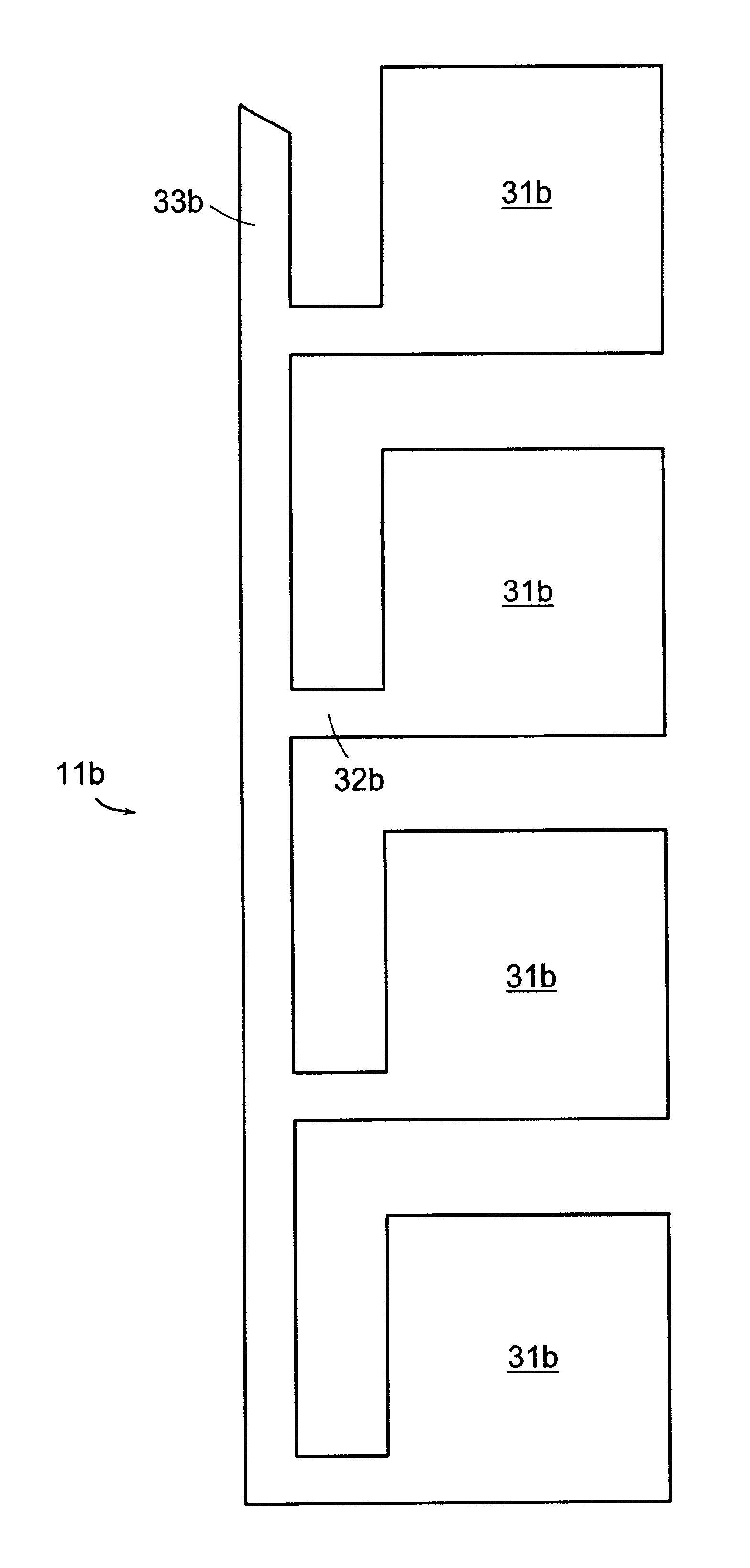
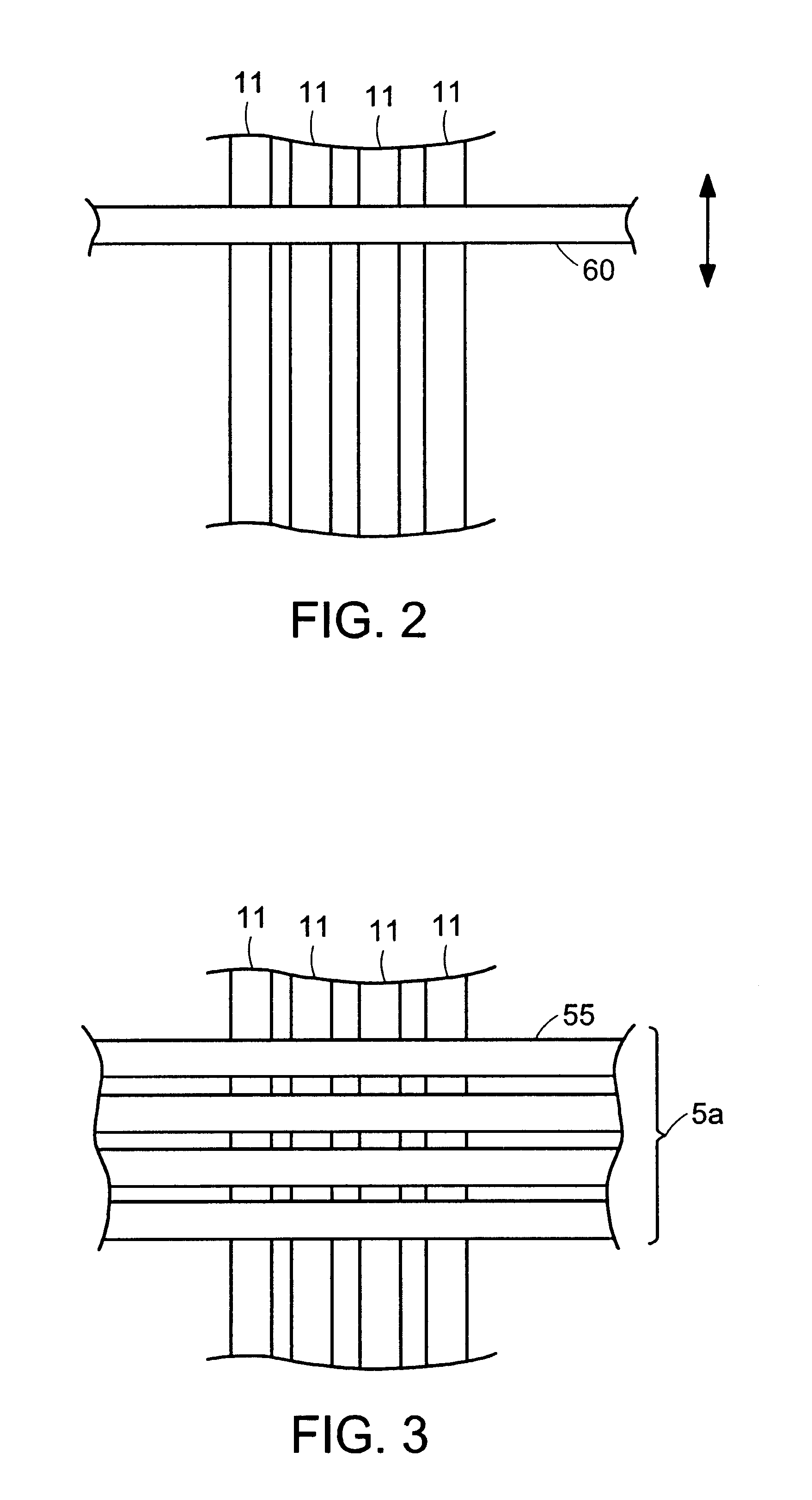
[0049]In general terms, the invention provides an apparatus and method for passive addressing of pixels in a display device. A “pixel” is herein understood to mean an individual element in an array of image elements. In particular, the invention overcomes difficulties inherent in addressing techniques that utilize orthogonally arranged rows and columns of electrodes in active or passive addressing. The invention permits use of display media previously unsuited for passively addressed displays.

[0050]Various embodiments of the invention, some of which are described in more detail in following sections, make use of voltage and light for matrix addressing of image elements in a display. Some embodiments require only one set of electrodes, e.g. a set of column electrodes. Display medium included in a pixel may have its optical state modified by coincident application of a voltage to an electrode that is adjacent to the display medium while illumination is applied to photoconductive mater...


PUM

PropertyMeasurementUnit
thicknessaaaaaaaaaa
thicknessaaaaaaaaaa
wavelength rangeaaaaaaaaaa

Abstract

The invention features a photoconductively addressed display and a method of photoconductive addressing in a display. The method includes providing an electro-optic imaging layer that extends in an X direction and a Y direction and comprises an array of image elements. A column electrode layer is provided adjacent to one side of the electro-optic imaging layer. The column electrode layer includes a plurality of column electrodes that each extend in the Y direction and are spaced from one another in the X direction. A photoconductive layer disposed between the electro-optic imaging layer and the column electrode layer is provided. An elongate portion of the photoconductive layer is illuminated in the X direction while scanning the illumination in the Y direction to translate a location of the illuminated elongate portion. At least one image element of the array of image elements is addressed by applying an intermittent voltage to one of the plurality of column electrodes that is adjacent to the at least one image element while the illuminated elongate portion of the photoconductive layer is adjacent to the at least one image element.

Description

FIELD OF THE INVENTION[0001]This invention relates generally to electro-optic displays. More particularly, the invention relates to systems for and methods of addressing electro-optic displays with a combined application of light and voltage.BACKGROUND OF THE INVENTION[0002]A number of interesting electro-optic display media have potential application in displays possessing good optical appearance, large area potential, flexible substrates, low cost, and ease of manufacture. Such display media include microencapsulated electrophoretic displays, rotating bichromal ball displays, suspended particle displays, and composites of liquid crystals with polymers, including polymer dispersed liquid crystals, polymer stabilized liquid crystals, and liquid crystal gels.[0003]Such display media also include electrochromic media. An example electrochromic medium takes the form of a nanochromic film including an electrode formed at least in part from a semiconducting metal oxide and dye molecules ...

Claims


Application Information

Patent Timeline
Patent Type & Authority Patents(United States)
IPC IPC(8): G02F1/13G02F1/1343G02F1/135
CPCG02F1/135G02F1/134336
Inventor MORRISON, IAN D.FORGIT, RACHAEL A.VALIANATOS, PETER J.HERB, CRAIG A.DANNER, GUY M.
Owner E INK CORPORATION
Why Eureka
Try Eureka