A kind of array substrate, liquid crystal panel and display device
A technology for array substrates and regions, applied in the field of liquid crystal panels and display devices, and array substrates, can solve the problems of increasing production costs, increasing production processes, and different lengths, and achieve the effects of reducing production costs and simplifying the production process
- Summary
- Abstract
- Description
- Claims
- Application Information
AI Technical Summary
Problems solved by technology
Method used
Image

Examples
Embodiment 1
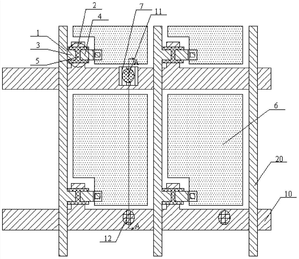
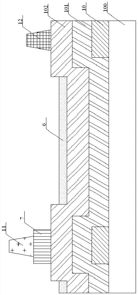
[0026] to combine figure 1 and figure 2 As shown, an array substrate is provided in an embodiment of the present invention, which includes a data line 20 and a gate line 10, and a plurality of pixel units defined by the data line 20 and the gate line 10, and each pixel unit includes a thin film transistor 1 and a pixel Electrode 6. The array substrate also includes a spacer and a spacer setting area, the spacer includes a main spacer 11 and an auxiliary spacer 12, and the spacer setting area includes a main spacer setting area and an auxiliary spacer In the spacer installation area, the main spacer 11 is arranged in the main spacer installation area, and the auxiliary spacer 12 is arranged in the auxiliary spacer installation area.
[0027] Wherein, the top surface of the main spacer arrangement area is higher than the top surface of the auxiliary spacer arrangement area, forming a certain height difference. The main spacer 11 is formed on the top surface of the main space...
Embodiment 2
[0043] The embodiment of the present invention also provides a liquid crystal panel, including an array substrate and a color filter substrate arranged in opposite boxes, and the color filter substrate includes a black matrix, wherein the array substrate adopts the array substrate in Embodiment 1, and the The spacer arrangement area on the array substrate corresponds to the position of the black matrix on the color filter substrate.
[0044] Since the spacer is formed on the array substrate, technical problems such as blue spots caused by the spacer formed on the color filter substrate are overcome, and the display quality of the liquid crystal panel is improved. At the same time, since the length of the main spacer and the auxiliary spacer are the same, they can be formed simultaneously through one patterning process, which simplifies the manufacturing process and reduces the production cost.
Embodiment 3
[0046] The embodiment of the present invention also provides a display device, which adopts the liquid crystal panel in the second embodiment, which improves the display quality of the display device and reduces the production cost of the product.
[0047] In the technical solution of the present invention, the main spacers and auxiliary spacers supporting the thickness of the liquid crystal panel box are formed on the array substrate, and the top surface of the main spacer installation area on the array substrate is higher than the auxiliary spacer installation area. The top surface of the spacer, and through this height difference to realize the level difference between the main spacer and the auxiliary spacer, so that the length of the main spacer and the auxiliary spacer can be designed to be the same, and can be formed simultaneously through a single patterning process, simplifying the Manufacturing process, reduce the production cost of the product.
PUM
 Abstract
Description
Claims
Application Information
 - R&D
- Intellectual Property
- Life Sciences
- Materials
- Tech Scout
- Unparalleled Data Quality
- Higher Quality Content
- 60% Fewer Hallucinations
Browse by: Latest US Patents, China's latest patents, Technical Efficacy Thesaurus, Application Domain, Technology Topic, Popular Technical Reports.
© 2025 PatSnap. All rights reserved.Legal|Privacy policy|Modern Slavery Act Transparency Statement|Sitemap|About US| Contact US: help@patsnap.com