Contact, semiconductor testing device, and semiconductor testing method

A test device and test method technology, applied in the direction of single semiconductor device testing, measuring devices, instruments, etc., can solve the problem of insufficient contact, and achieve the effects of suppressing scars, prolonging life, and reducing poor appearance

Active Publication Date: 2018-05-04
FUJI ELECTRIC CO LTD
View PDF10 Cites 0 Cited by
  • Summary
  • Abstract
  • Description
  • Claims
  • Application Information

AI Technical Summary

Problems solved by technology

Therefore, in a semiconductor testing device, even if a plurality of contacts are arranged so that the front ends of the contacts are arranged horizontally, there are cases where the contacts in one semiconductor device sufficiently contact some terminals but do not sufficiently contact other terminals. Happening

Method used


Image

  • Contact, semiconductor testing device, and semiconductor testing method
  • Contact, semiconductor testing device, and semiconductor testing method
  • Contact, semiconductor testing device, and semiconductor testing method

Examples


Embodiment Construction

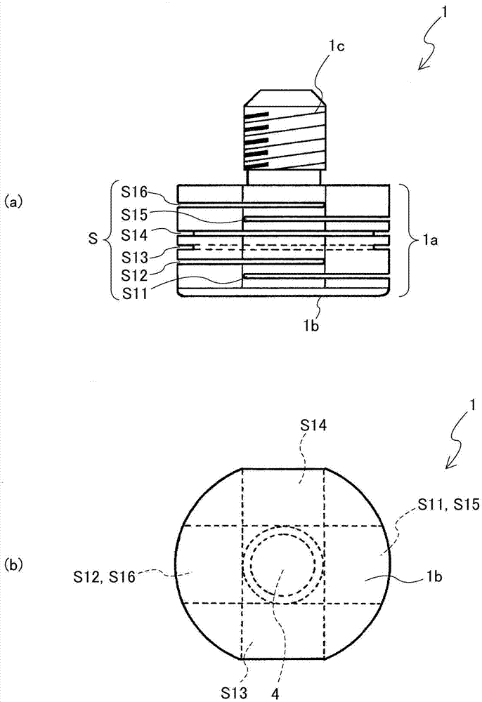
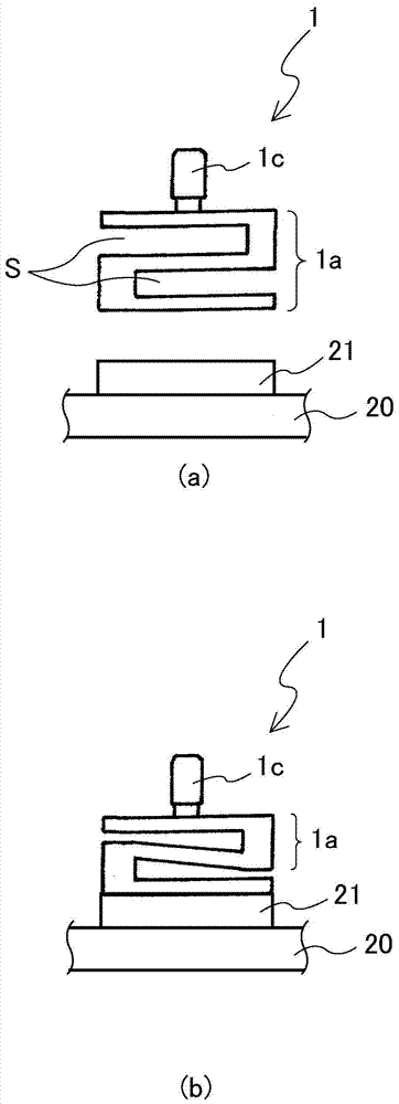
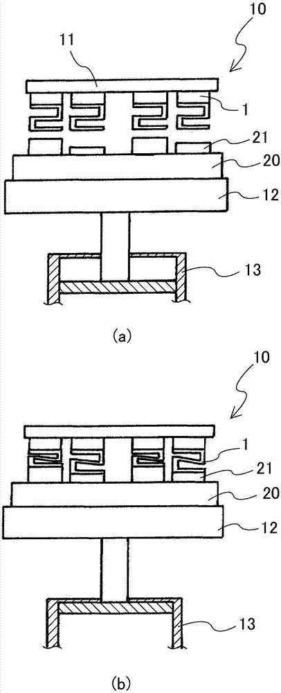
[0041] Hereinafter, embodiments of a contact and a semiconductor testing device according to the present invention will be specifically described with reference to the drawings.

[0042] figure 1 It is a front view of a semiconductor device test contact according to an embodiment of the present invention ( figure 1 (a)) and bottom view ( figure 1 (b)). figure 1 The illustrated contact 1 is made of a conductive metal material, and includes a deformed portion 1a having a columnar shape and a connecting portion 1c protruding from one end of the deformed portion 1a. In the illustrated example, the deformed portion 1a has a substantially cylindrical shape with a diameter substantially equal to the width dimension of the upper surface of the terminal of the semiconductor device. In one example, the diameter is about 13mm and the height is about 7mm. However, the size of the deformation portion 1a is not limited to the size limited to the illustrated example, and may be a siz...


PUM


Abstract

The present invention provides a semiconductor device testing contact capable of reducing contact resistance with a terminal of a semiconductor device and having a long life, a semiconductor testing device provided with the contact, and a semiconductor testing method using the contact. The contact of the present invention is a contact (1) for testing a semiconductor device which is used to contact and press a terminal (21) of a semiconductor device (20) to allow current to flow through the semiconductor device (20). The contact (1) is provided with a contact portion having a flat contact surface (1b) in contact with a terminal (21) of a semiconductor device (20), and a deformation portion (1a) which is in contact with a terminal (21) of a semiconductor device (20). 21) Elastic deformation when contacted and pressed.

Description

technical field [0001] The present invention relates to a contactor of a semiconductor testing device for conducting an electrical characteristic test of a semiconductor device, a semiconductor testing device provided with the contactor, and a testing method using the contactor. Background technique [0002] A power semiconductor module as a semiconductor device generally houses one or more power semiconductor chips in an insulating case, and exposes a plurality of terminals electrically connected to the power semiconductor chips, more specifically, external output terminals. to the outside of the housing above and / or on the sides, etc. Before the power semiconductor module is shipped, the electrical characteristic test of the power semiconductor module is carried out. The electrical characteristic test includes a test in which a large current flows through a semiconductor chip of a power semiconductor module. [0003] As an example of a semiconductor testing device for pe...

Claims


Application Information

Patent Timeline
Patent Type & Authority Patents(China)
IPC IPC(8): G01R31/26G01R1/067
Inventor 丸山真生小池幸司
Owner FUJI ELECTRIC CO LTD
Why Eureka
Try Eureka