Chip with built-in programmable circuit

A technology for programming circuits and chips, applied in circuits, electrical components, electric solid devices, etc., can solve the problems of precision drop, packaging offset effect, stress generation, etc., and achieve the effect of improving accuracy and avoiding offset effect

Active Publication Date: 2017-10-20
WUXI ZGMICRO ELECTRONICS CO LTD
View PDF6 Cites 0 Cited by
  • Summary
  • Abstract
  • Description
  • Claims
  • Application Information

AI Technical Summary

Problems solved by technology

However, for analog circuits with high precision, even if the calibration is more accurate before packaging, the thermal effect of the package will generate stress, which will lead to package shift effect, and the package will lead to a decrease in accuracy.

Method used


Image

  • Chip with built-in programmable circuit
  • Chip with built-in programmable circuit
  • Chip with built-in programmable circuit

Examples


Embodiment Construction

[0020] In order to make the above objectives, features and advantages of the present invention more obvious and understandable, the present invention will be further described in detail below with reference to the accompanying drawings and specific embodiments.

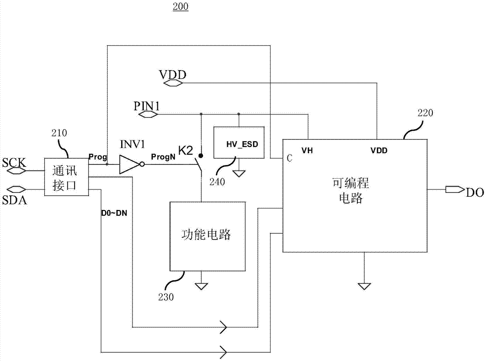
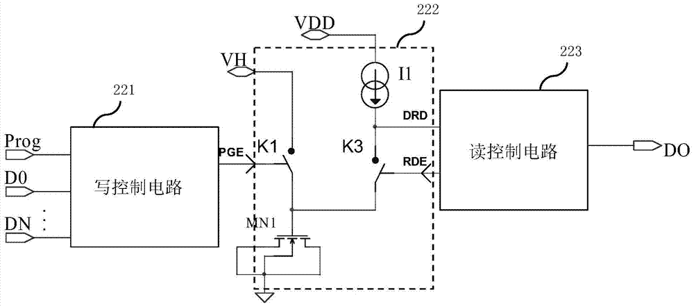
[0021] The present invention provides an improved chip with a built-in programmable circuit, which can realize programming or trimming after packaging. figure 2 The schematic circuit diagram of the chip 200 with built-in programmable circuit of the present invention in an embodiment is shown. image 3 for figure 2 A schematic circuit diagram of the programmable circuit 220 in one embodiment.

[0022] Such as figure 2 As shown, the chip 200 includes a programmable pin PIN1, communication pins SCK and SDA, a communication interface 210 connected to the communication pins SCK and SDA, and a programmable circuit 220.

[0023] Combine reference image 3 As shown, the programmable circuit 220 includes a programmable terminal V...


PUM


Abstract

The invention provides a chip with a built-in programmable circuit. The chip comprises a programmable pin, a communication pin, a communication interface and the programmable circuit, wherein the communication interface is connected with the communication pin, the programmable circuit comprises a programmable end and one or more programmable unit(s), the programmable end is connected with the programmable pin, each programmable unit comprises a first control switch and a programmable device, one end of the first control switch is connected with the programmable end, and the other end of the first control switch is connected with the programmable device. When a valid programmable mode signal is received, the voltage of a programming power supply is accessed to the programmable pin; and when the programmable unit is required to be programmed, the programmable circuit controls the first control switch to be switched on, and the voltage of the programming power supply can break down the programmable device. Therefore, programming can be still achieved after package, the accuracy after programming is improved, and the shift effect brought by package is avoided.

Description

【Technical Field】 [0001] The invention relates to the field of chip design, in particular to a chip with a built-in programmable circuit. 【Background technique】 [0002] In various circuit systems, programmable circuits are more and more widely used, which can improve the applicability of the chip to different applications. A programmable circuit is often integrated in a digital circuit, or an analog circuit or a digital-analog hybrid circuit. Traditional programmable circuits such as figure 1 As shown, it can be a metal fuse or a polysilicon fuse. The fuse includes a guide part and a fuse part, and two ends of the fuse are respectively connected to pads PAD1 and PAD2. Because programming a programmable circuit generally requires a higher current, it is generally fuse by means of probes after the wafer is manufactured and before packaging. However, for high-precision analog circuits, even if the calibration is more accurate before packaging, the thermal effect of the package w...

Claims


Application Information

Patent Timeline
Patent Type & Authority Patents(China)
IPC IPC(8): H01L23/49H01L27/112
Inventor 王钊
Owner WUXI ZGMICRO ELECTRONICS CO LTD
Why Eureka
Try Eureka