A voltage conversion control method, device and flash memory

A technology of voltage conversion and control method, applied in static memory, read-only memory, information storage, etc., can solve the problems of reducing the erasing and writing efficiency, increasing the voltage conversion time, etc., to achieve the effect of improving the erasing and writing efficiency

Active Publication Date: 2019-10-18
GIGADEVICE SEMICON (BEIJING) INC
View PDF2 Cites 0 Cited by
  • Summary
  • Abstract
  • Description
  • Claims
  • Application Information

AI Technical Summary

Problems solved by technology

[0005] It can be seen that the traditional flash memory has a leakage problem during the erasing / programming process, and the bleeding increases the voltage conversion time during the erasing / programming process, that is, the period when the original voltage changes from a high voltage to another high voltage , will increase the waiting time between an enable signal VPPI_EN being pulled down and turned on again, thus reducing the erasing efficiency

Method used


Image

  • A voltage conversion control method, device and flash memory
  • A voltage conversion control method, device and flash memory
  • A voltage conversion control method, device and flash memory

Examples


Embodiment 1

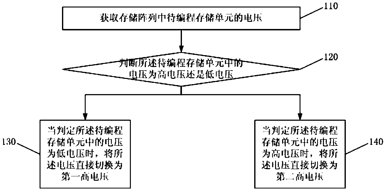
[0042] refer to figure 2 As shown, Embodiment 1 of the present invention provides a flow chart of a voltage conversion control method, the control method including:

[0043] Step 110, acquiring the voltage of the memory cell to be programmed in the memory array.

[0044] As mentioned above, the memory array includes a plurality of memory cells arranged in an array, and each memory cell is composed of a word line and a bit line, wherein the drains of the memory cells in the same row or column are connected to the word line, and the same The gates of multiple memory cells in a row or in the same column are connected to the bit line, and the memory cell is also composed of a transistor. Since a memory cell is the smallest storage unit of the memory array, when data is written into the memory array, usually multiple memory cells are written, so at least one or at least one column / row of memory cells is usually programmed here.

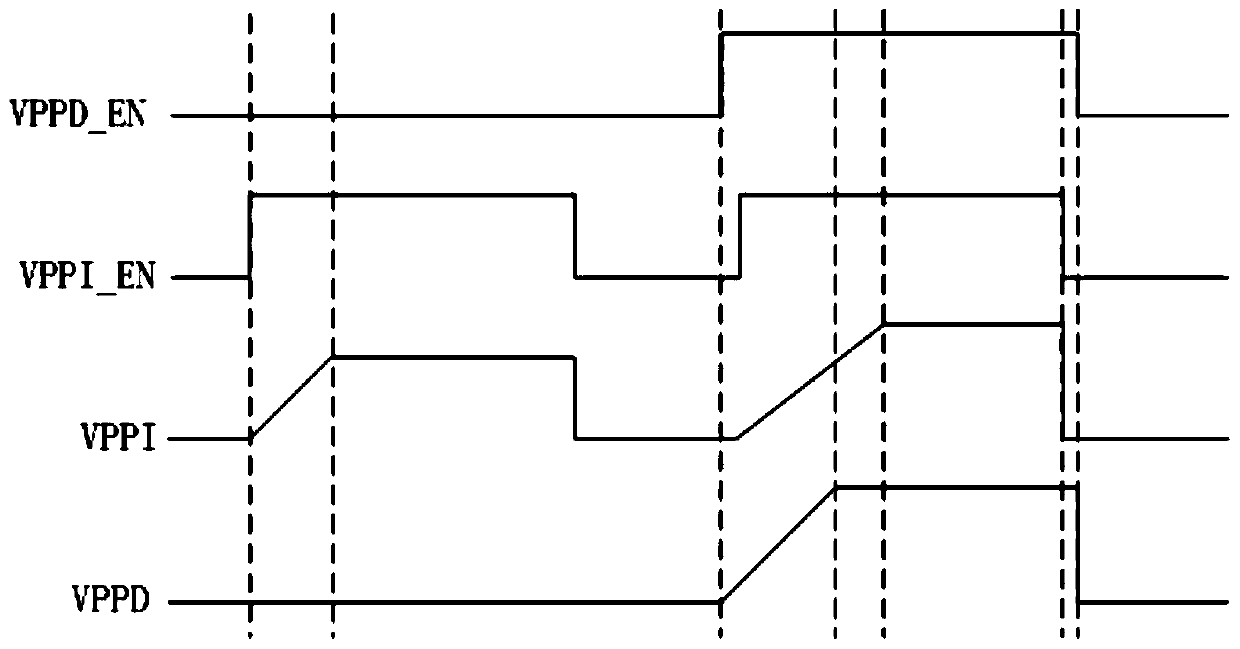
[0045]Known erasing / programming control circuit ad...

Embodiment 2

[0065] refer to image 3 , provides a schematic diagram of a voltage conversion control device according to Embodiment 2 of the present invention. The voltage conversion control device includes: a voltage acquisition module 210 , a voltage determination module 220 , a first switching module 230 and a second switching module 240 .

[0066] Among them, the obtaining voltage module 210 is used to obtain the voltage of the storage unit to be programmed in the storage array; the judging voltage module 220 is used to judge whether the voltage in the storage unit to be programmed is a high voltage or a low voltage; the first switching module 230, When it is determined that the voltage in the storage unit to be programmed is a low voltage, it is used to directly switch the voltage to the first high voltage; the second switching module 240, when it is determined that the voltage in the storage unit to be programmed is a high voltage When , it is used to directly switch the voltage to t...

Embodiment 3

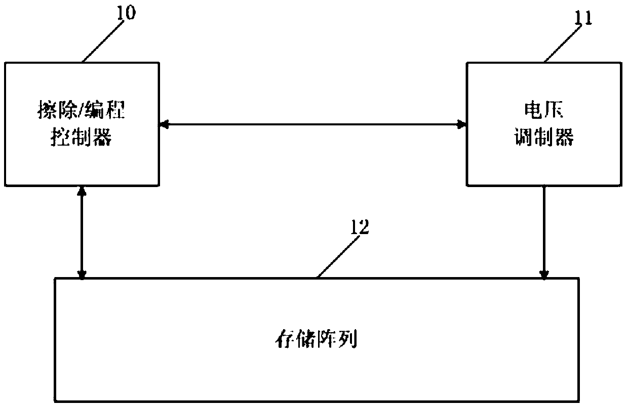
[0075]4(a) is a schematic diagram of a flash memory provided by Embodiment 3 of the present invention, the flash memory includes: a storage array 310, an erasing / programming control circuit 320, a voltage modulation circuit 340 and a voltage conversion control circuit 330, wherein the voltage conversion control circuit 330 is the voltage conversion control device described in Embodiment 2;

[0076] The memory array 310 includes a plurality of memory cells, wherein, as described above, the memory array 310 includes a plurality of memory cells arranged in an array, and the drains of the memory cells in one row or one column are connected to the same bit line, and the drains of the memory cells in one row or one column are connected to the same bit line. The gates of the memory cells are connected to the same word line, and any memory cell can be accurately addressed according to the address signal.

[0077] The erasing / programming control circuit 320 is used to address the stora...


PUM


Abstract

The invention discloses a control method and apparatus for voltage conversion and a flash memory. The control method for voltage conversion comprises the following steps: acquiring the voltage of a to-be-programmed memory cell in a memory array; determining whether the voltage of the to-be-programmed memory cell is high voltage or low voltage; and converting the voltage into first high voltage if it is determined that the voltage of the to-be-programmed memory cell is low voltage, or directly converting the voltage into second high voltage if it is determined that the voltage of the to-be-programmed memory cell is high voltage. According to the invention, the voltage of the to-be-programmed memory cell is determined; when the voltage is low voltage, the low voltage is directly converted into the first high voltage; and when the voltage is high voltage, the high voltage is directly converted into the second high voltage, so programming of the to-be-programmed memory cell is realized. The control method and apparatus for voltage conversion provided by the invention are capable of improving the erasing efficiency of the flash memory.

Description

technical field [0001] The invention relates to flash memory technology, in particular to a control method and device for voltage conversion and a flash memory. Background technique [0002] At present, flash memory has been gradually used in various electronic, digital, and intelligent products, such as portable multimedia players, mobile phones or notebook computers, etc. People's requirements for flash memory are getting higher and higher, such as good rewritable Erasing and writing efficiency is high. [0003] As shown in FIG. 1( a ), it is a schematic structural diagram of a flash memory provided in the prior art, and the flash memory includes an erase / program controller 10 , a voltage modulator 11 and a storage array 12 . The erasing / programming controller 10 selects the target storage unit corresponding to the address signal from the storage array 12 according to the address signal, and sends the voltage parameters of the addressed target storage unit to the power mo...

Claims


Application Information

Patent Timeline
Patent Type & Authority Patents(China)
IPC IPC(8): G11C16/06G11C16/02
Inventor 刘铭邓龙利张建军
Owner GIGADEVICE SEMICON (BEIJING) INC
Why Eureka
Try Eureka