Nonvolatile storage device and programming method thereof

A technology of non-volatile storage and programming methods, applied in static memory, read-only memory, information storage, etc., can solve the problems of complex and large overall power management solutions, reduce the area and increase the design complexity , Improve the effect of programming operations

Inactive Publication Date: 2017-04-26
WUHAN XINXIN SEMICON MFG CO LTD
View PDF5 Cites 0 Cited by
  • Summary
  • Abstract
  • Description
  • Claims
  • Application Information

AI Technical Summary

Problems solved by technology

[0005] The purpose of the present invention is to provide a non-volatile memory device and its programming method in which different word lines apply the same bypass voltage and the programming effect is not affected, so as to solve the overall power management scheme of the existing non-volatile memory device Large and complex problems

Method used


Image

  • Nonvolatile storage device and programming method thereof
  • Nonvolatile storage device and programming method thereof
  • Nonvolatile storage device and programming method thereof

Examples


Embodiment 1

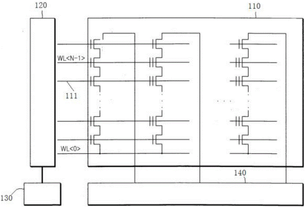
[0049] This embodiment provides a non-volatile storage device, the non-volatile storage device includes a memory cell array, a programming voltage generator, a bypass voltage generator, and a verification voltage generator, wherein: The memory cell array includes a number of word lines and a number of memory cells, each word line is connected to a plurality of memory cells, and the word lines are stacked and arranged; the programming voltage generator is connected to the memory cell array, and is The word line provides the programming voltage.

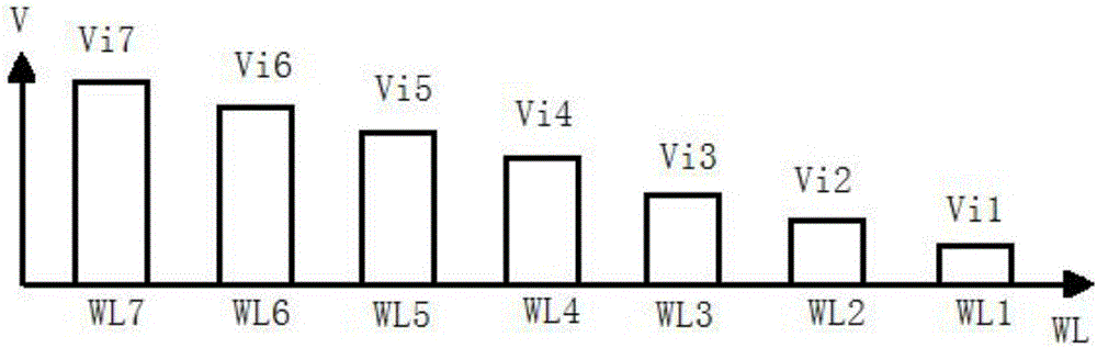
[0050] Figure 3 (a) is a schematic diagram of the programming voltage applied by the nonvolatile memory device of the present invention, WL7 ~ WL1, as the word line position increases, the amplitude of the programming voltage gradually decreases, the bypass voltage generator is connected to The memory cell array provides a bypass voltage for the word lines in the selected block in the memory cell array, which is different from the bypass ...

Embodiment 2

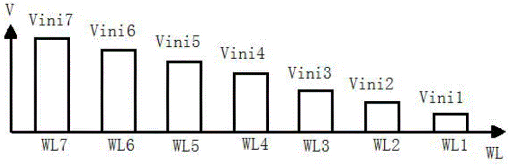
[0056] This embodiment provides a method for programming a non-volatile memory device, Figure 4 It is a flowchart of the method for programming a nonvolatile memory device of the present invention, such Figure 4 As shown, the non-volatile memory device programming method includes: inputting a programming instruction to the memory cell array; setting the programming voltage according to the position of the word line where the memory cell selected in the programming instruction is located; bypassing the voltage generator to the storage The same bypass voltage is applied to all word lines in the selected block in the cell array; the programming voltage generator applies the corresponding programming voltage to the word line where the selected memory cell is located to program the word line in the memory cell; The verification voltage is set at the position of the word line where the selected memory cell is located; the verification voltage generator applies a corresponding verific...


PUM


Abstract

The invention provides a nonvolatile storage device and a programming method thereof. The nonvolatile storage device comprises a storage unit array, a programming voltage generator, a bypass voltage generator and a calibration voltage generator, wherein the bypass voltage generator provides a bypass voltage for word lines in selected blocks in the storage unit array, and the voltage amplitudes of the bypass voltage in different word lines are equal. The programming method of the nonvolatile storage device comprises the steps that the same bypass voltage is exerted on the word lines in the storage unit array; a programming voltage is exerted on the word line where a selected storage unit is located; a calibration voltage is set according to the position of the word line where the selected storage unit is located; the corresponding calibration voltage is exerted on the word line where the selected storage unit is located, and calibration is performed. By exerting the same bypass voltage on different word lines, the bypass voltage generator does not need to be composed of multiple sets of voltage regulators and analog switches, therefore, an overall power management scheme is simplified, and the area is reduced.

Description

Technical field [0001] The present invention relates to the field of semiconductor technology, in particular to a non-volatile storage device and a programming method thereof. Background technique [0002] An electrically erasable / programmable nonvolatile memory device can retain data even when power supply is stopped, and a memory is a representative example of an electrically erasable / programmable nonvolatile memory device. In particular, the NAND type memory has a string structure in which a plurality of flash memory cells are connected in series, and therefore can be easily integrated and can be manufactured at low cost. For this reason, NAND-type flash memory has been used as a data transmitter for various types of portable products. [0003] figure 1 Is a schematic diagram of an existing non-volatile storage device, such as figure 1 As shown, the non-volatile memory device includes a memory cell array 110, a voltage generator and decoding and transmission circuit 120, a logi...

Claims


Application Information

Patent Timeline
Patent Type & Authority Applications(China)
IPC IPC(8): G11C16/10G11C16/08
CPCG11C16/10G11C16/08
Inventor 杨诗洋王颀付祥刘飞李婷郑世程夏志良霍宗亮
Owner WUHAN XINXIN SEMICON MFG CO LTD
Why Eureka
Try Eureka