
A multi-level selection structure applied to antifuse fpga

A technology of selecting structure and anti-fuse, applied in special data processing applications, architecture with a single central processor, electrical digital data processing, etc., can solve problems such as lack of radiation resistance and unsatisfactory

Active Publication Date: 2022-02-01
58TH RES INST OF CETC
View PDF5 Cites 0 Cited by
  • Summary
  • Abstract
  • Description
  • Claims
  • Application Information

AI Technical Summary

Problems solved by technology

Conventional civilian FPGAs do not have the ability to resist radiation, and cannot meet the needs of complex radiation environments such as aerospace and military industries.

Method used


Image

  • A multi-level selection structure applied to antifuse fpga
  • A multi-level selection structure applied to antifuse fpga
  • A multi-level selection structure applied to antifuse fpga

Examples


Embodiment 1

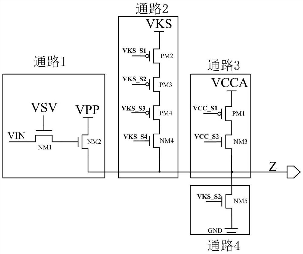
[0031] The invention provides a multi-level selection structure applied to antifuse FPGA. Such as figure 1 As shown, the multi-level selection structure includes 5 types of voltage sources, which are the programming voltage VPP of the antifuse, the voltage VSV for controlling the opening and closing of the programming pass transistor, and the voltage VKS for precharging the antifuse. (1 / 2 VPP, also called half programming voltage), the voltage VCCA used for normal operation after antifuse programming, has a low voltage GND, which provides low voltage for antifuse unit programming.

[0032] read on figure 1 , in the first channel 1, during the programming process of the antifuse, a programming voltage VPP is applied to one end of the antifuse to be programmed for high-voltage programming, and a conductive filament is formed inside the MTM antifuse unit, which can realize permanent conduction. The input signal VIN of the NMOS transistor NM1 comes from the upper level conversi...


PUM


Abstract

The invention discloses a multi-level selection structure applied to an antifuse FPGA, belonging to the technical field of integrated circuit design. The multi-level selection structure includes a first path, applying a programming voltage VPP to one end of the antifuse that needs to be programmed for high-voltage programming; a second path, providing a voltage VKS for an unprogrammed antifuse for pre-charging protection; Three channels, when the programming of the antifuse FPGA circuit is completed, the enable control signal turns on the charge pump circuit, and the output signal of the charge pump circuit turns on the third path to provide the working voltage VCCA for the unit connected to the antifuse; Four channels, when programming, apply a low voltage GND to the other end of the programmed antifuse to realize the programming of the antifuse. By using the multi-level selection structure applied to the anti-fuse FPGA provided by the present invention, the anti-fuse FPGA can flexibly perform programming, testing and normal operation modes, thereby improving the working efficiency of programming and testing circuits.

Description

technical field [0001] The invention relates to the technical field of integrated circuit design, in particular to a multi-level selection structure applied to an antifuse FPGA. Background technique [0002] FPGA (Field Programmable Gate Array, Field Programmable Gate Array) is a new type of device developed on the basis of PAL, GAL, CPLD and other programmable logic circuit devices, as a semi-customized Circuit, which has flexible and scalable architecture design technology, has large-capacity programmable logic resources and large-scale wiring resources, far exceeding the original programmable gate circuit. Because of its high integration, strong flexibility, low development cost, short development cycle, low risk, and high reliability, it has gradually replaced ASIC circuits in the field of system development and design. [0003] According to the internal programmable principle, the common mainstream FPGA circuit types mainly include SRAM type, anti-fuse type and FLASH t...

Claims


Application Information

Patent Timeline
Patent Type & Authority Patents(China)
IPC IPC(8): G06F30/331G06F30/343G06F15/78
CPCG06F15/7871
Inventor 蔺旭辉曹杨曹靓王晓玲
Owner 58TH RES INST OF CETC
Learn More