AMOLED panel and preparation method thereof

A panel and glass cover technology, applied in semiconductor/solid-state device manufacturing, organic light-emitting device manufacturing/processing, electrical components, etc., can solve problems such as abnormal key signals, characteristic degradation, and poor display of AMOLED panels

Active Publication Date: 2016-03-02
EVERDISPLAY OPTRONICS (SHANGHAI) CO LTD
View PDF3 Cites 5 Cited by
  • Summary
  • Abstract
  • Description
  • Claims
  • Application Information

AI Technical Summary

Problems solved by technology

However, under normal circumstances, the characteristics will be degraded by the influence of static electricity, so AMOLED panels need to have good packaging to isolate static electricity
[0003] In the current AMOLED panel, when the key signal line is connected, because the line is very thin, it is easy to damage the line by static electricity, which will cause abnormal key signal and cause poor display.
[0004] Therefore, a new process is urgently needed to solve the problem of poor display of AMOLED panels due to electrostatic damage to key signal lines.

Method used


Image

  • AMOLED panel and preparation method thereof
  • AMOLED panel and preparation method thereof

Examples


Embodiment 1

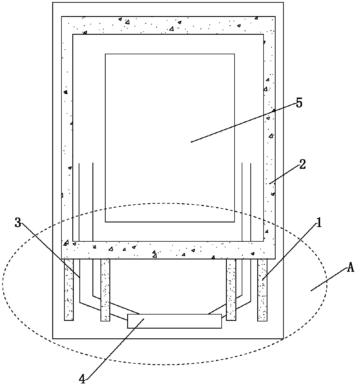
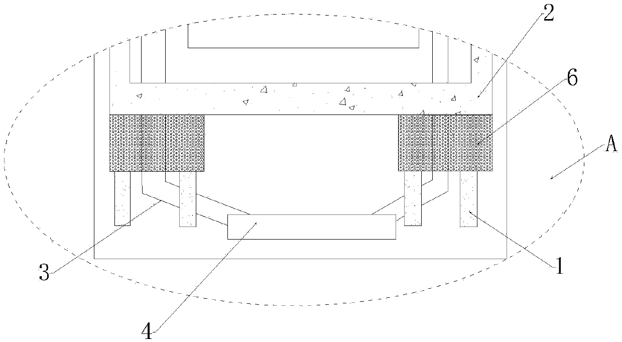
[0045] Figure 1-Figure 2 Shown is a schematic structural view of the AMOLED panel in the embodiment of the present application; as figure 1 As shown, in order to prevent the key signal lines in the current AMOLED panel from being damaged due to static electricity, the present invention designs a new AMOLED panel, wherein the specific operating areas are as follows: figure 1 As shown in the mark A, the invention includes:

[0046] An AMOLED panel body provided with a driver IC terminal 4 is provided with an image display area 5 on the AMOLED panel body, and a glass encapsulant 2 is coated around the image display area.

[0047] A number of power lines 1 are also arranged on the AMOLED panel body. In this embodiment, in order to better illustrate how the subsequent implementation is implemented, these power lines 1 are close to the edge of the AMOLED panel body, and the edges are all Two power lines are provided, and power lines 1 are provided on both side edges of the AMOLED...

Embodiment 2

[0053] The present application also provides a method for preparing an AMOLED panel, which can be applied to prepare the AMOLED panel mechanism described in the first embodiment above, and the method specifically includes:

[0054] First of all, the AMOLED panel body can be prepared based on the traditional preparation process, and the AMOLED panel body is provided with several signal lines, drive IC terminals and image display areas, and the several signal lines are mainly used for the transmission of key signals of the AMOLED panel. When the signal line is affected by external static electricity, it will seriously reduce the display quality of the entire display screen prepared subsequently, and even cause the entire display screen to fail to work normally. Next, prepare an insulating layer and lay it on the above-mentioned several signal lines. For example, the insulating layer can cover the exposed surface of the signal lines, so as to insulate each signal line from its adj...


PUM


Abstract

The invention relates to the field of semiconductor optimization and especially relates to an AMOLED panel and a preparation method thereof. A conducting layer is erected between power supply wires on two ends of the AMOLED panel, and further potential static electricity is shielded, so that key signal wires of a lower layer are protected against the influences of the static electricity, the key signal wires are enabled to normally transmit signals, and the purpose that the AMOLED panel is good in displaying performance is achieved.

Description

technical field [0001] The invention relates to the field of semiconductor optimization, in particular to an AMOLED panel and a preparation method thereof. Background technique [0002] With the continuous development of science and technology, people have higher and higher requirements for displays. OLED refers to the phenomenon that organic light-emitting materials emit light through carrier injection and recombination under the drive of an electric field. The principle of OLED light emission is to use ITO electrode and metal electrode as the anode and cathode of the device respectively. Under a certain voltage drive, electrons and holes are injected from the cathode and anode to the electron and hole transport layer respectively, and the electrons and holes pass through the electron and hole respectively. The hole transport layer migrates to the emissive layer, where they meet to form excitons and excite the luminescent molecules, which undergo radiative relaxation to em...

Claims


Application Information

Patent Timeline
Patent Type & Authority Applications(China)
IPC IPC(8): H01L27/32H01L51/56
CPCH10K59/131H10K71/00
Inventor 周兴雨
Owner EVERDISPLAY OPTRONICS (SHANGHAI) CO LTD
Why Eureka
Try Eureka