
A dual-band distribution and combining device
A dual-band, port technology, applied in the direction of connection devices, circuits, waveguide devices, etc., can solve the problems of inconvenient use, inability to isolate DC signals, and inability to take into account the working frequency forging, etc., to achieve circuit matching, improve stability, The effect of increasing safety
- Summary
- Abstract
- Description
- Claims
- Application Information
AI Technical Summary
Problems solved by technology
Method used
Image

Examples
Embodiment Construction
[0029] The present invention will be further described below in conjunction with the accompanying drawings.
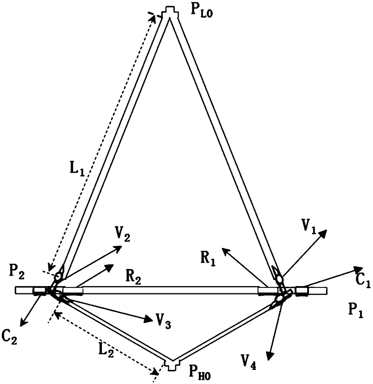
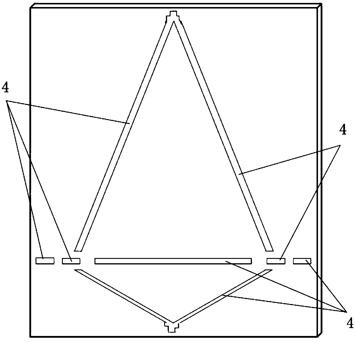
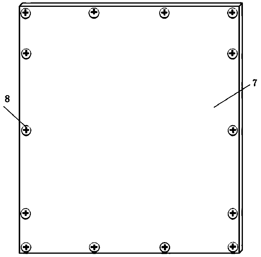
[0030] see Figure 4 and 5 , a dual-band distribution and combining device, including a metal cover 7 and a metal box 9, the metal box 9 is a rectangular block with an open top, such as image 3 shown. see image 3 and 5 , the metal cover plate 7 is assembled at the top opening of the metal box body 9, such as Figure 5 shown. see Figure 4 , one SMA connector 5 is respectively provided on the four walls of the metal box body 9 . see figure 1 , the four SMA connectors 5 are respectively marked as: P LO Port, P 1 Port, P 2 Port, P HO port, where P LO Port and P HO port relative, P 1 port at P LO Port and P HO Right side of port wiring, P 2 port at P LO Port and P HO Left side of port wiring.
[0031] see Figure 4 , a microstrip board is provided in the metal box body 9 . The microstrip plate is a rectangular plate. A DC blocking capacitor 1, a m...
PUM
 Abstract
Description
Claims
Application Information