a photodetector

A light detection and device technology, applied in the field of light detection devices, can solve problems such as failure, difficulty in capturing, and deviation of detection results, etc., to achieve the effects of improving accuracy, ensuring emission collimation, and preventing mutual interference

CN106298747BActive Publication Date: 2018-07-24NANTONG WELL ELECTRIC MOTOR
4 Cites 0 Cited by

Patent Information

Authority / Receiving Office
CN · China
Patent Type
Patents(China)
Current Assignee / Owner
Publication Date
2018-07-24

Smart Images

  • Figure 1
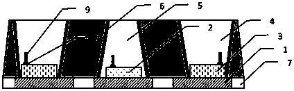
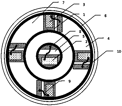
    Figure 1
  • Figure 2
    Figure 2
Patent Text Reader

Abstract

The invention provides an optical detector. A reflecting layer is used for separating a semiconductor chip for emitting radiation and a plurality of semiconductor chips for detecting radiation so as to ensure the independence of emission and detection, the mutual interference is prevented, and the detection accuracy is improved; and moreover, a first cavity in a circular table shape is used for emitting a radiation signal, and the emission collimation is ensured; and an annular cavity with an inverted isosceles trapezoid cross section is used as an accommodating cavity for radiation detecting, and thus, a feedback signal can be enabled to be received to the greatest extent.
Need to check novelty before this filing date? Find Prior Art

Description

technical field

[0001] The invention relates to the field of photodetection devices, in particular to a photodetection device with an injection molded housing, a radiation-emitting semiconductor chip and a radiation-detecting semiconductor chip. Background technique

[0002] It is known to design a component with a radiation-emitting semiconductor chip and a radiation-detecting semiconductor chip. However, the devices generally have semiconductor chips arranged in separate housings and spaced apart from one another, for example on a circuit board. However, the signal of the radiation-emitting semiconductor chip will affect the radiation-detecting semiconductor chip, resulting in deviation or failure of the detection result, and generally, the radiation-emitting signal is strong, while the feedback signal of the detection radiation is weak and difficult to capture. Contents of the invention

[0003] Based on solving the above-mentioned problems in the packaging, the presen...

Examples

Embodiment Construction

[0014] see figure 1 and 2 , the invention provides a photodetection device with an injection molded housing, a radiation-emitting semiconductor chip 2 and a plurality of radiation-detecting semiconductor chips 3, figure 2 4 semiconductor chips 3 are shown in , it can also be 6 or 8, etc., wherein a first cavity 4 and a second cavity 5 are formed in the injection molded housing, and the first cavity 4 is composed of an inner wall and a bottom The frustum-shaped cavity surrounded by the walls, the cross-section of the frustum-shaped cavity is an upright isosceles trapezoid, and the second cavity 5 is an annular cavity surrounded by the first cavity surrounded by the outer wall, the inner wall and the bottom wall. The section of the cavity is an inverted isosceles trapezoid; the bottom wall includes a plurality of conductive carriers 1 for carrying the radiation-emitting semiconductor chip 2 and a plurality of radiation-detecting semiconductor chips 3, a plurality of electrode ...