Module stain repairing device and method based on PC GPU

A repair method and module technology, applied in cathode ray tube indicators, instruments, static indicators, etc., can solve the problems of restricting the efficiency of modules to read Mura repair data, the long time of burning to FlashIC, and the unfavorable flat display mode Group production line repair and other issues to achieve the effect of improving Mura defect repair efficiency, saving SPI writing time, and flexible use

Active Publication Date: 2017-05-31
WUHAN JINGCE ELECTRONICS GRP CO LTD
View PDF7 Cites 12 Cited by
  • Summary
  • Abstract
  • Description
  • Claims
  • Application Information

AI Technical Summary

Problems solved by technology

[0004] First of all, due to the limitation of the BlockSize of the mura compensation chip of the flat-panel display module, the compensation accuracy of the compensated picture displayed in the above method is limited.
Secondly, at present, the Flash IC of the flat-panel display module to be repaired generally uses a single SPI bus for reading and writing. Due to the limitation of the bandwidth of the SPI bus, it takes a long time to burn the Mura repair data to the Flash IC. The process of writing data to Flash and then loading data from the Flash IC by the Mura compensation chip takes a long time, which is not conducive to the rapid repair of Mura defects in the flat-panel display module production line
These defects have a serious impact on the module's color spot repair effect, restricting the efficiency of the module in reading Mura repair data

Method used


Image

  • Module stain repairing device and method based on PC GPU
  • Module stain repairing device and method based on PC GPU
  • Module stain repairing device and method based on PC GPU

Examples


Embodiment Construction

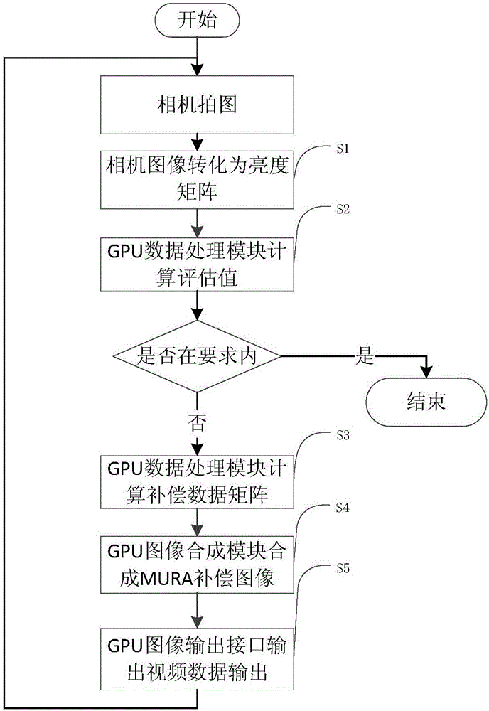
[0036] The present invention will be further described in detail below in conjunction with the accompanying drawings and specific embodiments.

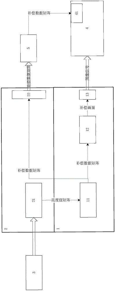
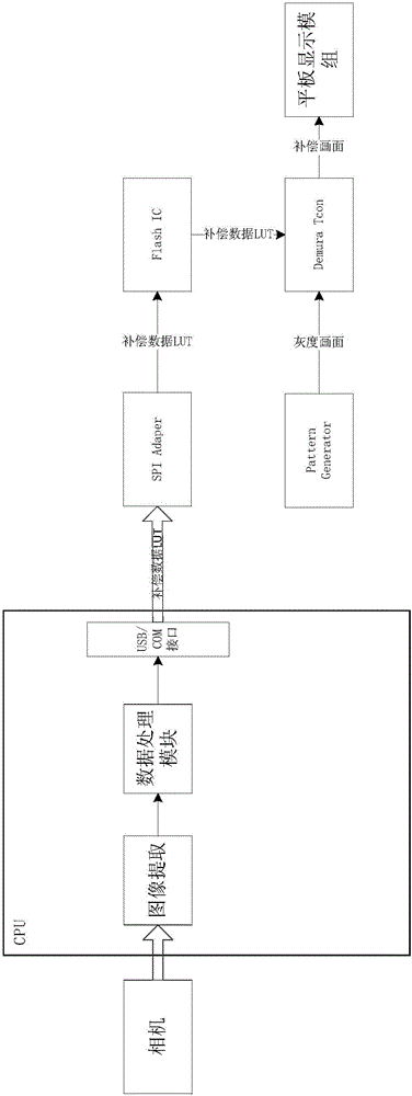
[0037] Such as figure 1 As shown, a kind of PC GPU-based module stain repairing device provided by the present invention includes a GPU data processing module 11, a GPU image synthesis module 12 and a GPU image output interface 13 arranged in the GPU1, and also includes a module arranged in the CPU2 The image extraction module 21 and the image transmission interface 22 in the.

[0038] The image extraction module 21 is used to obtain the data stream of the positioning picture and the picture to be repaired from the camera 3, and decode them into a matrix of brightness values ​​of the positioning picture and a matrix of brightness values ​​of the picture to be repaired, and send them to the GPU data processing module 11.

[0039] The image transmission interface 22 is used to obtain the Mura compensation image data from the GPU data p...


PUM


Abstract

The invention discloses a module stain repairing device and a module stain repairing method based on PC GPU. The device comprises a GPU data processing module, a GPU image synthesis module and a GPU image output interface, wherein the GPU data processing module acquires the picture mapping relation between a camera and a module by utilizing the parallel processing capability of GPU and according to the luminance value matrix of a located image picture, calculates the Mura assessed value of a to-be-repaired picture, judges that whether the gray scale luminance of the to-be-repaired picture satisfies the demands or not, and calculates the Mura compensation data matrix of the to-be-repaired picture; the GPU picture synthesis module is used for synthesizing the Mura compensation data matrix and the luminance value matrix of the to-be-repaired picture, thus forming a Mura compensation image; the GPU picture output interface is used for converting the Mura compensation image into image signal video stream which is sent to the module. According to the device and the method provided by the invention, PC GPU can directly generate and output Mura compensation picture signals, the Mura repairing data does not need to be written into a Flash IC of the to-be-repaired flat display module, but the to-be-repaired flat display module can display the display effect after Mura repairing, and thus the repairing efficiency for the Mura defect of the flat display module production line is promoted.

Description

technical field [0001] The invention relates to the field of flat panel display, in particular to a PC GPU-based module stain repair device and method. Background technique [0002] Flat panel displays are currently widely used in consumer electronic products that people use daily, such as televisions, computers, mobile phones, and tablets. The flat-panel display module is the main component of the flat-panel display. Its manufacturing process is complex and requires multiple processes. Therefore, various display defects will inevitably occur during the manufacturing process, and these display defects are more common Mura (color spot) defects. The mura defect is that under the same light source and the same background color, different colors or differences in brightness are visually perceived, which brings visual discomfort to people and seriously affects the quality of flat-panel displays. [0003] At present, there are relevant technologies specifically aimed at repairing...

Claims


Application Information

Patent Timeline
Patent Type & Authority Applications(China)
IPC IPC(8): G09G3/20G09G5/10
CPCG09G3/2007G09G5/10G09G2320/0233
Inventor 刘钊郑增强沈亚非李苗黎国进
Owner WUHAN JINGCE ELECTRONICS GRP CO LTD
Why Eureka
Try Eureka