Check patentability & draft patents in minutes with Patsnap Eureka AI!

Nand flash memory storage unit, nand flash memory and method for forming same

A technology of flash storage and flash memory, which is applied in the field of NAND flash memory storage units, and can solve problems such as high production costs

Active Publication Date: 2019-10-18
SHANGHAI FUDAN MICROELECTRONICS GROUP
View PDF4 Cites 0 Cited by
  • Summary
  • Abstract
  • Description
  • Claims
  • Application Information

AI Technical Summary

Problems solved by technology

[0011] However, in the existing three-dimensional NAND flash memory, the reading reliability of the memory cell array needs to be improved, the data density needs to be improved, and the manufacturing cost is high

Method used


Image

  • Nand flash memory storage unit, nand flash memory and method for forming same
  • Nand flash memory storage unit, nand flash memory and method for forming same
  • Nand flash memory storage unit, nand flash memory and method for forming same

Examples


Embodiment Construction

[0077] As mentioned in the background, in the existing three-dimensional NAND flash memory, the reading reliability of the memory cell array needs to be improved, and the data density needs to be improved.

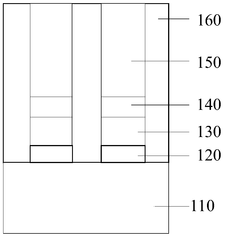
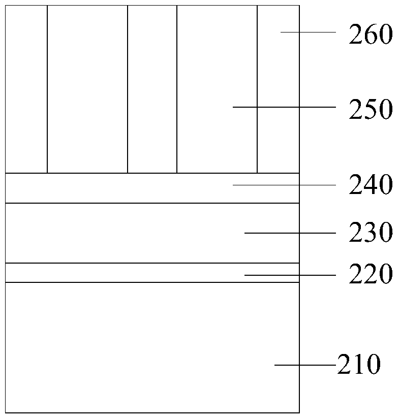
[0078] For this reason, the present invention provides a kind of new NAND flash storage unit, and described NAND flash memory storage unit comprises semiconductor substrate; The first fin portion that is positioned at described semiconductor substrate; To the first stacked isolation layer, the first stacked structure, the second isolation layer and the second stacked structure; the first stacked structure includes a first source layer, a first channel layer and a first drain layer; The second stack structure includes a second source layer, a second channel layer and a second drain layer. The first source layer, the first channel layer and the first drain layer of the NAND flash memory storage unit are vertically stacked, therefore, the NAND flash memory storage unit has a ...


PUM


Abstract

A NAND flash memory storage unit, a NAND flash memory and a forming method thereof. The NAND flash storage unit includes: a semiconductor substrate; a first fin located on the semiconductor substrate; the first fin at least includes a first isolation layer stacked from bottom to top, a first stack structure, A second isolation layer and a second stack structure; the first stack structure includes a first source layer, a first channel layer, and a first drain layer; the second stack structure includes a second source layer, a second channel layer and second drain layer. The NAND flash storage unit has a good capability of continuously shrinking the process size, and the NAND flash storage unit can solve the problem of memory unit read disturbance from the device structure. At the same time, the method for forming the NAND flash memory is simple, and the process cost is reduced.

Description

technical field [0001] The invention relates to the field of semiconductor manufacturing, in particular to a NAND flash memory storage unit, a NAND flash memory and a forming method thereof. Background technique [0002] NAND flash memory (NAND flash) is a kind of non-volatile flash memory. Its main function is to store data. It has high storage cell density and fast writing and erasing speed. At the same time, the storage cell size of NAND flash memory is almost the same as that of NOR flash memory storage cell. It can provide higher capacity within a given mold size, and is currently mainly used in digital camera flash memory cards and MP3 players. [0003] A kind of storage unit of existing NAND flash memory such as figure 1 As shown, there is a channel layer 110 on a semiconductor substrate (not shown), and a tunneling dielectric layer 120, a floating gate 130, a gate dielectric layer 140, and a control gate 150 are sequentially arranged on the channel layer 110, and th...

Claims


Application Information

Patent Timeline
Patent Type & Authority Patents(China)
IPC IPC(8): H01L27/11524H10B41/35
CPCH10B41/35
Inventor 黄新运肖磊刘红霞徐烈伟沈磊刘崎
Owner SHANGHAI FUDAN MICROELECTRONICS GROUP
Features
  • R&D
  • Intellectual Property
  • Life Sciences
  • Materials
  • Tech Scout
  • Unparalleled Data Quality
  • Higher Quality Content
  • 60% Fewer Hallucinations
Learn More