A kind of array substrate and preparation method thereof

An array substrate and scanning line technology, applied in the field of semiconductor display, can solve problems affecting the performance of thin film transistors, and achieve the effect of improving display quality and improving conduction efficiency

Active Publication Date: 2020-03-10
SHENZHEN CHINA STAR OPTOELECTRONICS SEMICON DISPLAY TECH CO LTD
View PDF3 Cites 0 Cited by
  • Summary
  • Abstract
  • Description
  • Claims
  • Application Information

AI Technical Summary

Problems solved by technology

However, since copper atoms are easy to diffuse between the films, when metal copper is used as electrode lines and electrodes, copper atoms will diffuse into the active layer of the thin film transistor, thereby affecting the performance of the thin film transistor

Method used


Image

  • A kind of array substrate and preparation method thereof
  • A kind of array substrate and preparation method thereof
  • A kind of array substrate and preparation method thereof

Examples


Embodiment Construction

[0066] The following will clearly and completely describe the technical solutions in the embodiments of the present invention in conjunction with the accompanying drawings in the embodiments of the present invention. In the description and the drawings of the description, the same structures use the same symbols. Obviously, the described embodiments are only the present invention. Some, but not all, embodiments of the invention. Based on the embodiments of the present invention, all other embodiments obtained by persons of ordinary skill in the art without making creative efforts belong to the protection scope of the present invention.

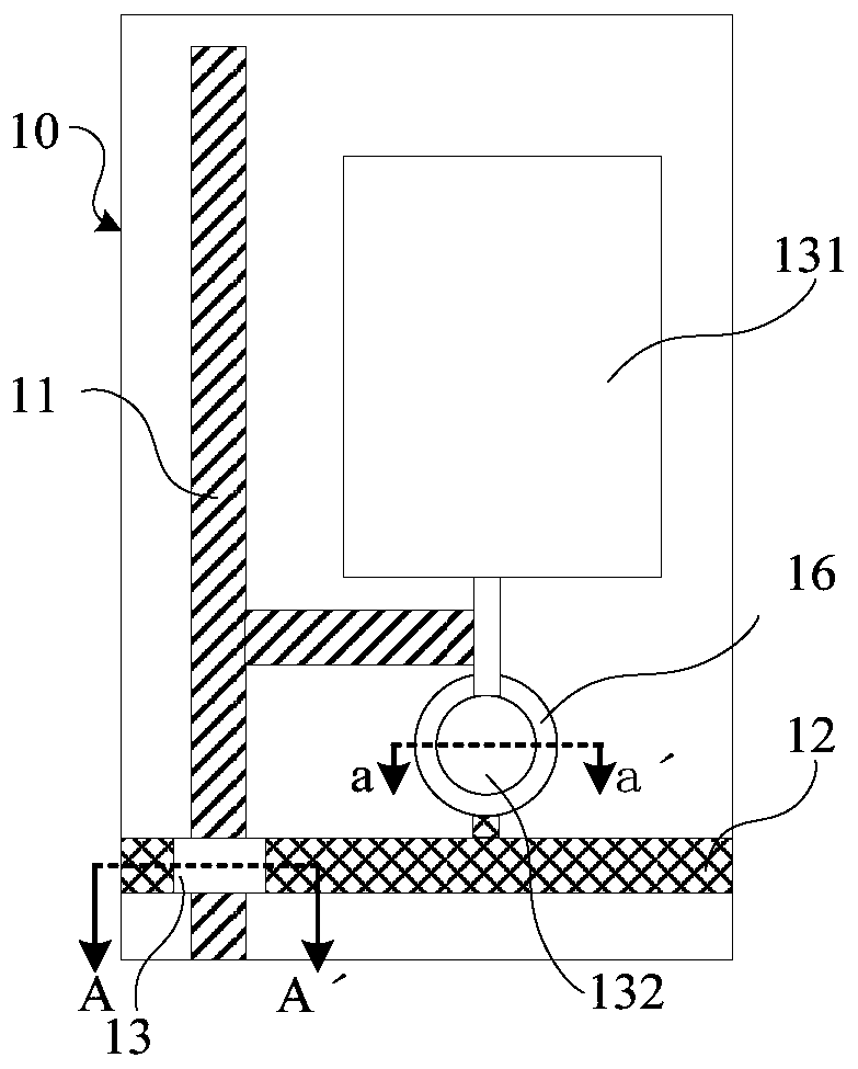
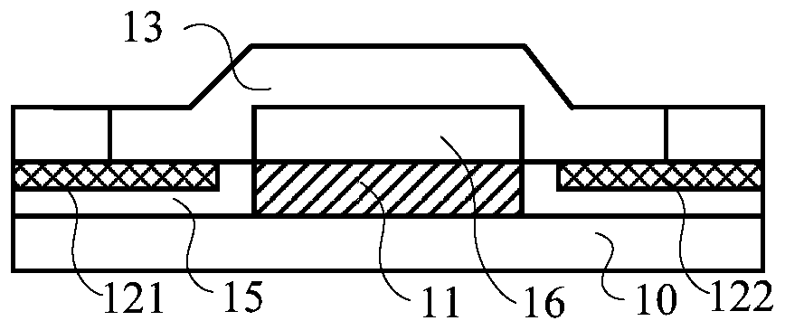
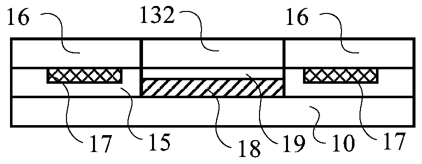
[0067] refer to figure 1 , Figure 2a and Figure 2b , figure 1 is a top view of an embodiment of the array substrate of the present invention, Figure 2a yes figure 1 The shown array substrate is a cross-sectional view along A-A′ in an application example (corresponding to the part of the data line 11), Figure 2b yes figure 1 The show...


PUM


Abstract

The invention discloses an array substrate and a preparation method therefor. The preparation method comprises the steps: forming a data line, a graphene source electrode and a grid insulating layer on the array substrate; forming a scanning line and a grid electrode on the grid insulating layer; forming a passivation layer on the data line, the scanning line and the grid electrode, and carrying out the ion implantation for the graphene source electrode, so as to convert a part of the graphene source electrode into a semiconductor active layer; respectively forming a drain electrode and an ITO pixel electrode on the semiconductor active layer. Through the above mode, the method employs the graphene for the preparation of the graphene source electrode and the semiconductor active layer, can make the most of the high conductivity of graphene, and improves the conduction efficiency of the array substrate.

Description

technical field [0001] The present invention relates to the technical field of semiconductor display, in particular to an array substrate and a preparation method thereof. Background technique [0002] With the continuous development of semiconductor display technology, the display panel has higher and higher requirements on the conductivity of the electrode lines on the array substrate and the electrodes of the thin film transistors. Especially in high-resolution products, in order to increase the aperture ratio, it is necessary to reduce the line width of the electrode lines on the basis of ensuring electrical conductivity; resistance. [0003] In the prior art, metals such as metal copper or metal aluminum are usually used as the electrode lines in the array substrate and the electrodes in the thin film transistors, which can easily achieve low line width, low power consumption and high conductivity, thereby improving the performance of the display panel. display effect...

Claims


Application Information

Patent Timeline
Patent Type & Authority Patents(China)
IPC IPC(8): H01L27/12H01L29/45
CPCH01L27/124H01L27/127H01L29/45
Inventor 周志超
Owner SHENZHEN CHINA STAR OPTOELECTRONICS SEMICON DISPLAY TECH CO LTD
Why Eureka
Try Eureka