Thin film transistor and manufacturing method thereof, display panel and display apparatus

A thin-film transistor and display panel technology, applied in the direction of transistors, semiconductor/solid-state device manufacturing, semiconductor devices, etc., can solve the problems of poor electrical characteristics, reduce the electrical characteristics of thin-film transistors, and display adverse effects, so as to improve electrical characteristics and reduce defects effect of density

Active Publication Date: 2018-08-31
YUNGU GUAN TECH CO LTD
View PDF3 Cites 0 Cited by
  • Summary
  • Abstract
  • Description
  • Claims
  • Application Information

AI Technical Summary

Problems solved by technology

[0002] In the display panel, a thin film transistor is provided to realize the control function in the display process. If the electrical characteristics of the thin film transistor are poor, it may cause adverse effects on the display.
In the current manufacturing process of thin film transistors, the structural defect density of thin film transistors will increase, thereby reducing the electrical characteristics of thin film transistors.

Method used


Image

  • Thin film transistor and manufacturing method thereof, display panel and display apparatus
  • Thin film transistor and manufacturing method thereof, display panel and display apparatus
  • Thin film transistor and manufacturing method thereof, display panel and display apparatus

Examples


Embodiment Construction

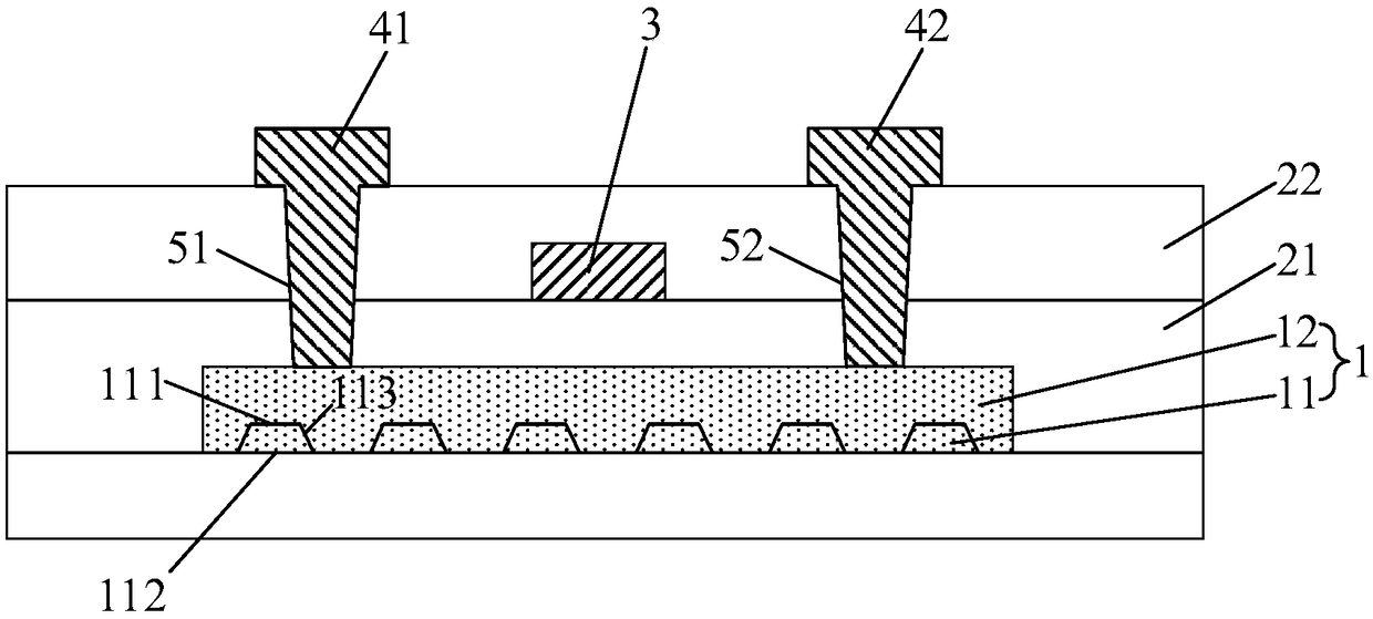
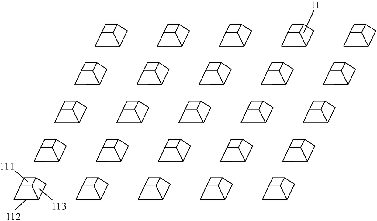
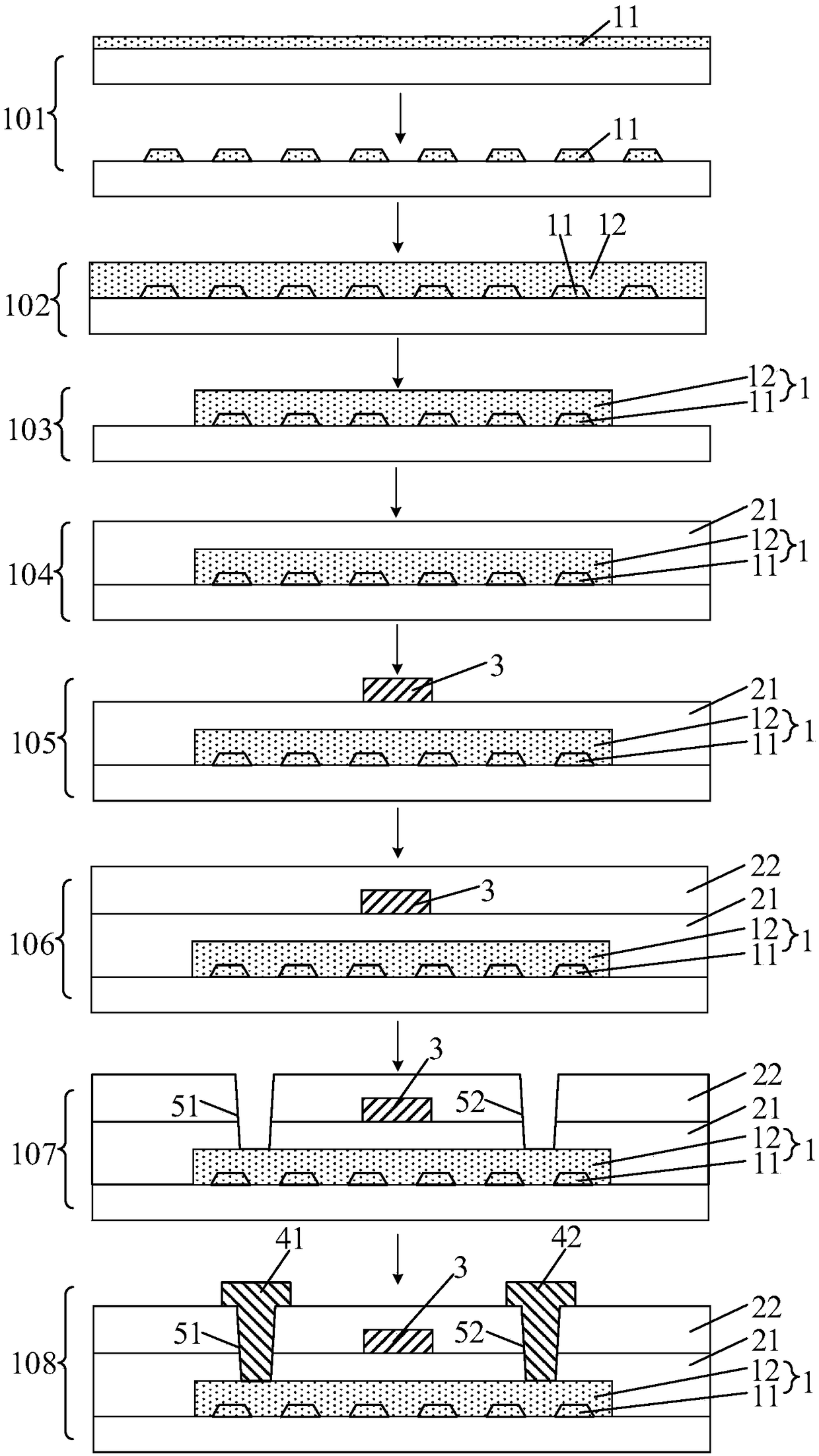
[0039] In order to make the purpose, technical solutions and advantages of the embodiments of the present invention clearer, the technical solutions in the embodiments of the present invention will be clearly and completely described below in conjunction with the drawings in the embodiments of the present invention. Obviously, the described embodiments It is a part of embodiments of the present invention, but not all embodiments. Based on the embodiments of the present invention, all other embodiments obtained by persons of ordinary skill in the art without creative efforts fall within the protection scope of the present invention.

[0040] Terms used in the embodiments of the present invention are only for the purpose of describing specific embodiments, and are not intended to limit the present invention. As used in the embodiments of the present invention and the appended claims, the singular forms "a", "said" and "the" are also intended to include the plural forms unless th...


PUM


Abstract

Embodiments of the invention provide a thin film transistor and a manufacturing method thereof, a display panel and a display apparatus, relate to the technical field of display, and can lower the structural defect density of the thin film transistor and improve electrical characteristic of the thin film transistor. The thin film transistor comprises an active layer, a first insulating layer, a gate, a second insulating layer, a source and a drain, wherein the active layer comprises a first semiconductor layer and a second semiconductor layer; the first semiconductor layer comprises a plurality of first island-shaped structures which are arranged at intervals; the second semiconductor layer covers the first semiconductor layer and the gaps among the multiple first island-shaped structures;the source is connected to the active layer through source via holes in the first insulating layer and the second insulating layer; and the drain is connected to the active layer through drain via holes in the first insulating layer and the second insulating layer.

Description

technical field [0001] The invention relates to the field of display technology, in particular to a thin film transistor, a manufacturing method thereof, a display panel and a display device. Background technique [0002] In the display panel, a thin film transistor is provided to realize the control function during the display process. If the electrical characteristics of the thin film transistor are poor, it may cause adverse effects on the display. During the manufacturing process of the current thin film transistor, the structural defect density of the thin film transistor will be increased, thereby reducing the electrical characteristics of the thin film transistor. Contents of the invention [0003] The invention provides a thin film transistor and its manufacturing method, a display panel and a display device, which can reduce the structural defect density of the thin film transistor, thereby improving the electrical characteristics of the thin film transistor. [...

Claims


Application Information

Patent Timeline
IPC IPC(8): H01L29/786H01L21/336H01L29/10
CPCH01L29/1033H01L29/66742H01L29/786H01L2021/775
Inventor 黄振
Owner YUNGU GUAN TECH CO LTD
Why Eureka
Try Eureka