a pixel arrangement

A pixel arrangement and seed pixel technology, applied in semiconductor devices, electrical components, circuits, etc., can solve the problems of OLED pixel arrangement and compensation, and achieve the effect of simple structure and easy realization

Active Publication Date: 2020-11-24
EVERDISPLAY OPTRONICS (SHANGHAI) CO LTD
View PDF5 Cites 0 Cited by
  • Summary
  • Abstract
  • Description
  • Claims
  • Application Information

AI Technical Summary

Problems solved by technology

[0004] The present invention provides a pixel arrangement, which is used to solve the problem that the prior art cannot provide an OLED pixel arrangement capable of compensating the OLED edge pixel display

Method used


Image

  • a pixel arrangement
  • a pixel arrangement
  • a pixel arrangement

Examples


Embodiment Construction

[0043]In order to make the object, technical solution and advantages of the present invention clearer, the present invention will be further described in detail below in conjunction with the accompanying drawings. Obviously, the described embodiments are only some embodiments of the present invention, rather than all embodiments . Based on the embodiments of the present invention, all other embodiments obtained by persons of ordinary skill in the art without making creative efforts belong to the protection scope of the present invention.

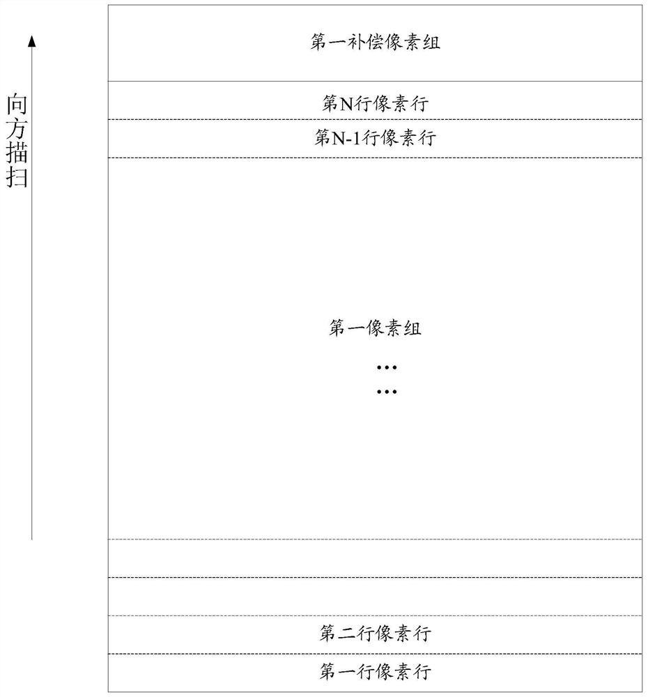
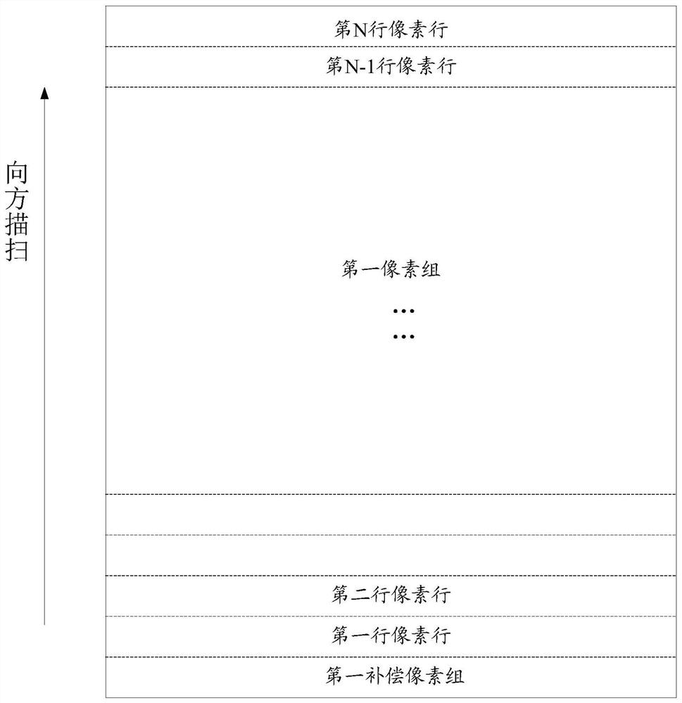
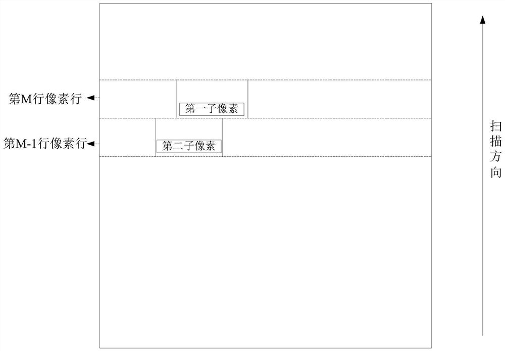
[0044] The present invention provides a pixel arrangement, such as figure 1 As shown, the pixel arrangement includes the first compensation pixel group and the first pixel group; the first pixel group includes the first to Nth rows of pixel rows in the scanning direction, wherein there is at least one first pixel in the pixel unit of the Mth row of pixels There is a compensation relationship between the sub-pixel and the second sub-pixel of...


PUM


Abstract

The present invention provides a pixel arrangement, including a first compensation pixel group and a first pixel group; the first pixel group includes the first to Nth pixel rows in the scanning direction, and there is at least one pixel unit in the Mth pixel row There is a compensation relationship between a sub-pixel and the second sub-pixel of the pixel unit in the M-1th row of pixel rows during display, the first sub-pixel and the second sub-pixel are the same sub-pixel, N is greater than 1, and M belongs to N; the first The compensation pixel group is adjacent to the edge pixel row in the first pixel group; there is at least one third sub-pixel in the first compensation pixel group and the fourth sub-pixel of the pixel unit of the edge pixel row has a compensation relationship during display; the second The third sub-pixel and the fourth sub-pixel are the same sub-pixel, and the fourth sub-pixel is the furthest away from the third sub-pixel in the pixel unit to which it belongs; the edge pixel row is the first pixel row or the Nth row in the first pixel group pixel row. The problem of color shift in the display of edge pixels in the prior art is solved.

Description

technical field [0001] The invention relates to the technical field of light emitting diode display, in particular to a pixel arrangement. Background technique [0002] In flat panel display technology, Organic Light-Emitting Diode (OLED) displays are famous for their thinness, active light emission, fast response speed, wide viewing angle, rich colors and high brightness, low power consumption, and high and low temperature resistance. It is recognized by the industry as the third generation of display technology after liquid crystal display (LCD). According to the driving method, OLED is divided into passive OLED (Passive Matrix OLED, PMOLED) and active OLED (Active Matrix OLED, AMOLED). PMOLED is also called passive matrix OLED, and AMOLED is also called active matrix OLED. PMOLED can only To produce small-sized, low-resolution display panels, AMOLED can realize large-sized, high-resolution panels because it integrates a thin-film transistor (TFT) and a capacitor in each ...

Claims


Application Information

Patent Timeline
Patent Type & Authority Patents(China)
IPC IPC(8): H01L27/32
CPCH10K59/121
Inventor 刘子涵陈郁仁
Owner EVERDISPLAY OPTRONICS (SHANGHAI) CO LTD
Why Eureka
Try Eureka