Display substrate, manufacturing method thereof, and display device

A technology for display panels and display devices, which can be used in semiconductor/solid-state device manufacturing, electrical components, and electrical solid-state devices, etc., and can solve problems such as device reliability and life decline, and OLED display device electrode corrosion.

Active Publication Date: 2019-03-29
BOE TECH GRP CO LTD +1
View PDF8 Cites 2 Cited by
  • Summary
  • Abstract
  • Description
  • Claims
  • Application Information

AI Technical Summary

Problems solved by technology

[0003] However, OLED display devices have problems such as electrode corrosion caused by oxygen and water vapor, resulting in reduced reliability and lifetime of the device

Method used


Image

  • Display substrate, manufacturing method thereof, and display device
  • Display substrate, manufacturing method thereof, and display device
  • Display substrate, manufacturing method thereof, and display device

Examples


Embodiment Construction

[0033] In order to make the above objects, features and advantages of the present invention more comprehensible, the present invention will be further described in detail below in conjunction with the accompanying drawings and specific embodiments.

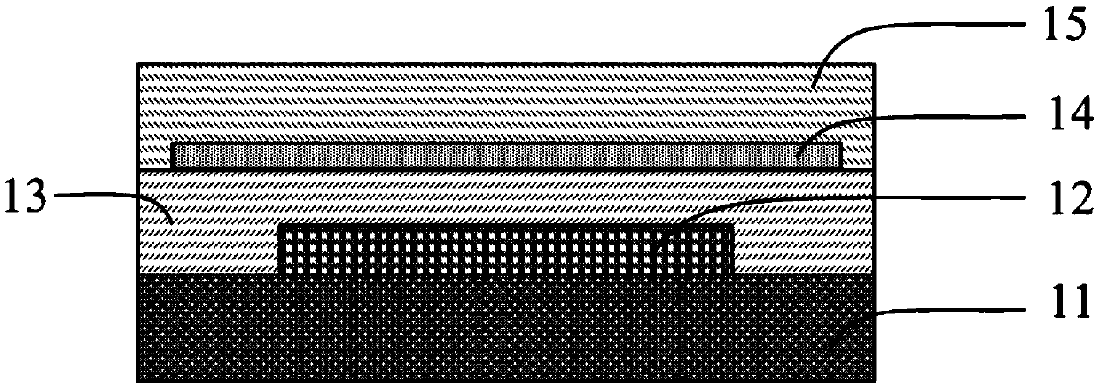
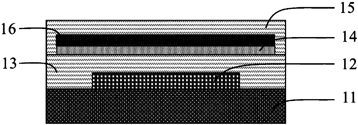
[0034] An embodiment of the present application provides a display panel, referring to figure 1 , the display panel may include: a substrate 11, and an OLED device 12 disposed on one side of the substrate 11; a first thin film encapsulation layer 13 disposed on the side of the OLED device 12 away from the substrate 11; disposed on the first thin film encapsulation layer 13 away from the substrate The water-absorbing oxygen storage layer 14 on the side of 11; the second film encapsulation layer 15 arranged on the side of the water-absorbing oxygen-storage layer 14 away from the substrate 11; wherein the water-absorbing oxygen-storage layer 14 can absorb water vapor and oxygen inside the display panel.

[0035] Specifically, the sub...


PUM

PropertyMeasurementUnit
Thicknessaaaaaaaaaa
Thicknessaaaaaaaaaa

Abstract

The invention provides a display panel, a preparation method thereof and a display device, and the display panel comprises a substrate and an OLED device arranged at one side of the substrate; a firstthin film packaging layer which is arranged at one side, deviating from the substrate, of the OLED device; a water absorption and oxygen storage layer which is arranged at one side, deviating from the substrate, of the first thin film packaging layer; a second film packaging layer which is arranged at one side, deviating from the substrate, of the water absorption and oxygen storage layer, wherein the water absorption and oxygen storage layer can absorb water vapor and oxygen in the display panel. According to the technical scheme, the water absorption and oxygen storage layer is arranged toabsorb water vapor and oxygen in the display panel, the water vapor and the oxygen can be effectively prevented from entering the OLED device, so the problems of electrode corrosion and the like caused by the water vapor and the oxygen are solved. Therefore, the reliability and the service life of the display device can be improved.

Description

technical field [0001] The invention relates to the field of display technology, in particular to a display panel, a manufacturing method thereof, and a display device. Background technique [0002] Organic light emitting diode (Organic Light Emitting Diode, hereinafter referred to as OLED) display device uses OLED to emit light of different brightness. Compared with traditional liquid crystal display device, OLED display device has faster response speed, higher contrast ratio and wider Viewing angle is an important development direction of display devices. [0003] However, OLED display devices have problems such as electrode corrosion caused by oxygen and water vapor, resulting in reduced reliability and lifetime of the device. Contents of the invention [0004] The invention provides a display panel, a manufacturing method thereof, and a display device, so as to improve the reliability and lifespan of the display device. [0005] In order to solve the above problems, ...

Claims


Application Information

Patent Timeline
IPC IPC(8): H01L51/52H01L51/56
CPCH10K50/846H10K50/844H10K71/00
Inventor 刘承俊胡贵光鲁俊祥孙少君尹君垚胡松
Owner BOE TECH GRP CO LTD
Why Eureka
Try Eureka