A kind of flexible electronic device and preparation method thereof

A technology of flexible electronic devices and electronic devices, applied in the direction of electrical solid devices, semiconductor/solid device manufacturing, electrical components, etc., can solve problems such as strain damage and performance degradation, and achieve enhanced flexible connections, improved performance and reliability, and improved Effect of Radiation Resistance Properties

Active Publication Date: 2022-06-07
SHANGHAI INST OF MICROSYSTEM & INFORMATION TECH CHINESE ACAD OF SCI
View PDF5 Cites 0 Cited by
  • Summary
  • Abstract
  • Description
  • Claims
  • Application Information

AI Technical Summary

Problems solved by technology

[0004] The purpose of the present invention is to solve the problem of performance degradation caused by strain damage in the preparation process of flexible silicon-on-insulator devices in the prior art

Method used


Image

  • A kind of flexible electronic device and preparation method thereof
  • A kind of flexible electronic device and preparation method thereof
  • A kind of flexible electronic device and preparation method thereof

Examples


Embodiment Construction

[0029] The technical solutions in the embodiments of the present application will be clearly and completely described below with reference to the accompanying drawings in the embodiments of the present application. Obviously, the described embodiments are only a part of the embodiments of the present application, but not all of the embodiments. Based on the embodiments in this application, all other embodiments obtained by those of ordinary skill in the art without creative work fall within the protection scope of this application.

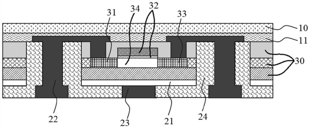
[0030] Reference herein to "one embodiment" or "an embodiment" refers to a particular feature, structure, or characteristic that may be included in at least one implementation of the present application. In the description of the present application, it should be understood that the orientation or positional relationship indicated by the terms "upper", "lower", "top", "bottom", etc. is based on the orientation or positional relationship shown in t...


PUM


Abstract

The present invention relates to the field of semiconductor technology, in particular to a flexible electronic device and a preparation method thereof, including: a flexible substrate and an electronic device, the electronic device includes a substrate layer and an extension layer, and the extension layer is arranged on the substrate layer; The flexible base is disposed on the surface of the extension layer away from the base layer. Forming a flexible substrate on the front of the electronic device can avoid mechanical failure and damage caused by device thinning, transfer, bonding and other manufacturing processes, and improve the performance reliability and stability of the flexible device. A large-area flexible isolation layer is formed between electronic devices to further enhance the flexible connection between device units and improve the overall flexibility and ductility of the device structure. The invention simultaneously forms a back gate bias control terminal, which can realize dynamic modulation of the electrical performance of the device and improve the anti-radiation characteristic of the device.

Description

technical field [0001] The invention relates to the technical field of semiconductors, in particular to a flexible electronic device and a preparation method thereof. Background technique [0002] In recent years, with the continuous development of electronic circuits, nanotechnology, materials, and artificial intelligence technologies, flexible electronic devices are considered to be "an important development direction of future electronic products". Flexibility of electronic devices can subvert the rigid physical form of traditional information devices. It has the characteristics of thinness, portability, implantability, and wearability, and can realize the efficient integration of information with people, objects and the environment. Flexible electronic device is an emerging electronic technology that makes organic and inorganic material electronic devices on flexible or ductile plastic or thin metal substrates. With its unique flexibility and ductility as well as efficie...

Claims


Application Information

Patent Timeline
Patent Type & Authority Patents(China)
IPC IPC(8): H01L23/31H01L21/768
CPCH01L23/3128H01L21/76898
Inventor 常永伟董业民刘艳吕凯
Owner SHANGHAI INST OF MICROSYSTEM & INFORMATION TECH CHINESE ACAD OF SCI
Why Eureka
Try Eureka