All-dielectric metasurface terahertz photoconductive antenna based on embedded metal nanostructure

A metal nanostructure, photoconductive antenna technology, applied in the field of terahertz photoconductive antennas, can solve the problems of low radiation power and conversion efficiency of terahertz photoconductive antennas, so as to improve radiation power and conversion efficiency, reduce transmission distance, reduce reflection effect

Pending Publication Date: 2021-03-19
XI'AN INST OF OPTICS & FINE MECHANICS - CHINESE ACAD OF SCI
View PDF0 Cites 1 Cited by
  • Summary
  • Abstract
  • Description
  • Claims
  • Application Information

AI Technical Summary

Problems solved by technology

[0018] The purpose of the present invention is to solve the disadvantages of low radiation power and conversion efficiency of terahertz photoconductive antennas in the prior art, and provide a kind of all-dielectric metasurface terahertz photoconductive antenna based on embedded metal nanostructures

Method used


Image

  • All-dielectric metasurface terahertz photoconductive antenna based on embedded metal nanostructure
  • All-dielectric metasurface terahertz photoconductive antenna based on embedded metal nanostructure
  • All-dielectric metasurface terahertz photoconductive antenna based on embedded metal nanostructure

Examples


Embodiment Construction

[0052] Below in conjunction with accompanying drawing and specific embodiment content of the present invention is described in further detail:

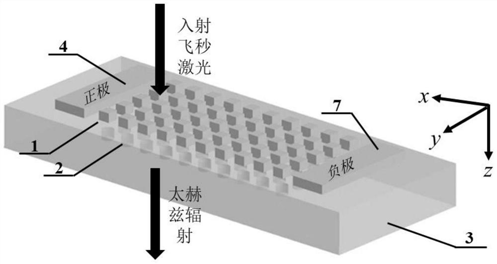
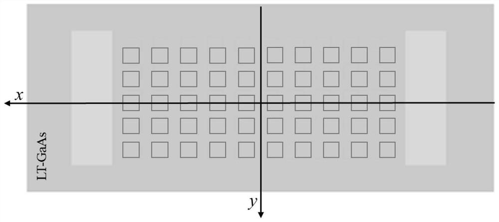
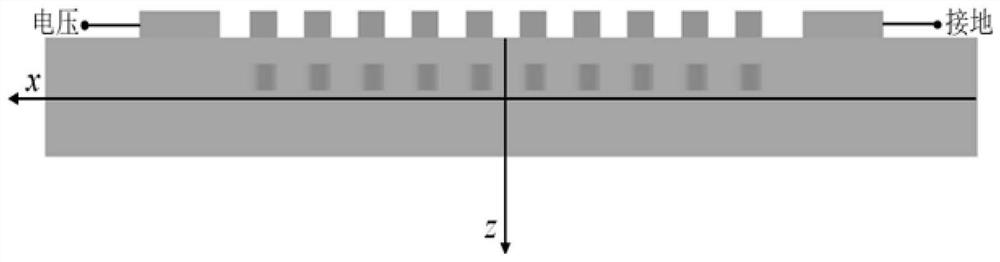
[0053] An all-dielectric metasurface terahertz photoconductive antenna based on embedded metal nanostructures, including a semiconductor substrate 3 , an all-dielectric anti-reflection metasurface array 1 , a metal nanostructure array 2 , and a metal positive electrode 4 and a metal negative electrode 7 . Among them, the all-dielectric antireflective metasurface array 1, the metal positive electrode 4 and the metal negative electrode 7 are all arranged on the upper surface of the semiconductor substrate 3 (when in use, the metal positive electrode applies a voltage, and the metal negative electrode is grounded), and the all-dielectric antireflective metasurface array 1 is located on the metal surface. Between the positive pole 4 and the metal negative pole 7, the metal positive pole 4 is connected to a voltage, and the metal negative p...


PUM

PropertyMeasurementUnit
diameteraaaaaaaaaa
heightaaaaaaaaaa
reflectanceaaaaaaaaaa

Abstract

The invention provides an all-dielectric metasurface terahertz photoconductive antenna based on an embedded metal nanostructure. The all-dielectric metasurface terahertz photoconductive antenna basedon the embedded metal nanostructure solves the problems that in the prior art, a terahertz photoconductive antenna generates terahertz waves, and the radiation power and the conversion efficiency arelow. The antenna comprises a semiconductor substrate, an all-dielectric anti-reflection metasurface array, a metal nanostructure array, a metal positive electrode and a metal negative electrode, wherein the all-dielectric anti-reflection metasurface array, the metal positive electrode and the metal negative electrode are arranged on the upper surface of the semiconductor substrate, and the all-dielectric anti-reflection metasurface array is located between the metal positive electrode and the metal negative electrode; the metal nanostructure array is arranged in the semiconductor substrate, and a distance exists between the metal nanostructure array and the upper surface of the semiconductor substrate.

Description

technical field [0001] The invention belongs to a terahertz photoconductive antenna, in particular to an all-dielectric metasurface terahertz photoconductive antenna based on an embedded metal nanostructure. Background technique [0002] Terahertz (THz) waves are electromagnetic radiation with a frequency between microwave and infrared bands, usually defined as electromagnetic waves with a frequency of 100GHz-10THz [1] . [0003] The unique spectral position of the terahertz wave makes it have the advantages of broadband, transmission and low energy, and has important application value in the fields of broadband communication, medical imaging, non-destructive testing and security inspection. [2] . [0004] As an important artificial terahertz source, terahertz photoconductive antenna (THz-PCA) can emit broadband terahertz radiation (covering the entire terahertz frequency band). It has important applications in material analysis and so on. [0005] The photoconductive an...

Claims


Application Information

Patent Timeline
Patent Type & Authority Applications(China)
IPC IPC(8): H01Q15/00H01Q1/36H01Q1/00H01Q1/52G01N21/3586
CPCG01N21/3586H01Q1/002H01Q1/364H01Q1/52H01Q15/0086
Inventor 范文慧江晓强宋超陈徐吴奇
Owner XI'AN INST OF OPTICS & FINE MECHANICS - CHINESE ACAD OF SCI
Why Eureka
Try Eureka