Display panel and display device

A display panel and display area technology, which is applied to semiconductor devices, electrical components, circuits, etc., to achieve the effects of saving process, improving light transmittance, and reducing manufacturing costs

Pending Publication Date: 2021-12-21
WUHAN TIANMA MICRO ELECTRONICS CO LTD
View PDF0 Cites 2 Cited by
  • Summary
  • Abstract
  • Description
  • Claims
  • Application Information

AI Technical Summary

Problems solved by technology

However, there is still no relevant solution for how to improve the light transmittance of the optical component area and simplify the process in the scheme of LTPO with optical components under the screen.

Method used


Image

  • Display panel and display device
  • Display panel and display device
  • Display panel and display device

Examples


Embodiment Construction

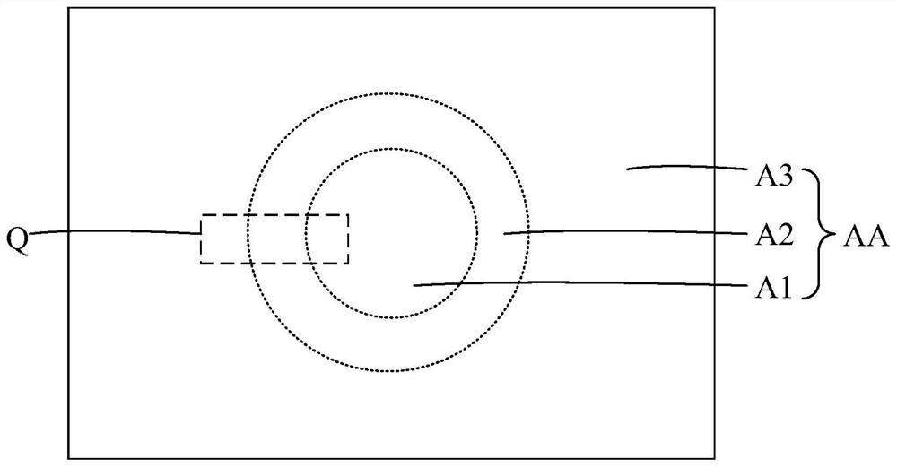
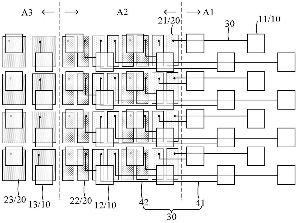
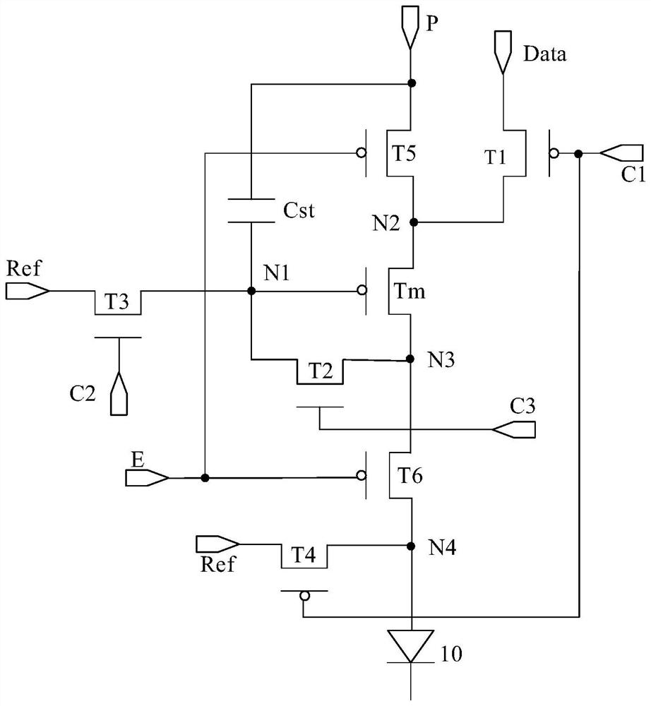
[0026] In order to make the purpose, technical solutions and advantages of the embodiments of the present invention clearer, the technical solutions in the embodiments of the present invention will be clearly and completely described below in conjunction with the drawings in the embodiments of the present invention. Obviously, the described embodiments It is a part of embodiments of the present invention, but not all embodiments. It will be apparent to those skilled in the art that various modifications and variations can be made in the present invention without departing from the spirit or scope of the inventions. Therefore, the present invention is intended to cover the modifications and variations of the present invention falling within the scope of the corresponding claims (technical solutions to be protected) and their equivalents. It should be noted that, the implementation manners provided in the embodiment of the present invention may be combined with each other if the...


PUM


Abstract

The invention provides a display panel and a display device. A display area of the display panel comprises an optical component area, a transition area and a first display area. The display area comprises a light-emitting device and a pixel circuit, and the light-emitting device comprises a first light-emitting device located in the optical component area. The pixel circuit comprises a first pixel circuit located in the transition area. The first light-emitting device is electrically connected with the first pixel circuit through a connecting line. The pixel circuit comprises a first transistor and a second transistor, an active layer of the first transistor is located on a first silicon semiconductor layer, and an active layer of the second transistor is located on a second metal oxide semiconductor layer. The connecting line comprises a first line segment and a second line segment which are mutually connected, the first line segment is located in the optical component area, and the second line segment is located in the transition area. The connecting line comprises a first connecting line, and the first line segment in the first connecting line is located on the second metal oxide semiconductor layer. The light transmittance of the optical component area can be improved, meanwhile, the technological process can be saved, and the manufacturing cost can be reduced.

Description

technical field [0001] The present invention relates to the field of display technology, in particular to a display panel and a display device. Background technique [0002] In electronic products such as mobile phones and tablet computers, optical components such as front cameras and infrared sensing elements occupy a certain amount of space on the front of the product and affect the screen-to-body ratio. With the introduction of the full screen concept in the display field, major manufacturers are making efforts in the field of full screen research. At present, it is generally believed that the under-screen optical component solution is a better solution that can realize a true full screen. The optical components such as the camera are arranged under the display area, and the position of the camera can be displayed normally. When the camera needs to be used, the light penetrates the display panel to reach the camera and is finally used by the camera. [0003] The electron...

Claims


Application Information

Patent Timeline
Patent Type & Authority Applications(China)
IPC IPC(8): H01L27/12H01L27/32
CPCH01L27/1214H01L27/1222H01L27/1225H01L27/124H10K59/00H10K59/12
Inventor 代好王磊王淼
Owner WUHAN TIANMA MICRO ELECTRONICS CO LTD
Why Eureka
Try Eureka