Organic electroluminescent device, manufacturing method thereof and electronic equipment
What is AI technical title?
AI technical title is built by Patsnap AI team. It summarizes the technical point description of the patent document.
a technology manufacturing methods, applied in the field of display technology, can solve the problems of high driving voltage, low efficiency, and top-emitting organic electroluminescent devices, and achieve the effect of improving the efficiency and lifetime of organic electroluminescent devices
Active Publication Date: 2018-10-30
BOE TECH GRP CO LTD +1
View PDF28 Cites 0 Cited by
Summary
Abstract
Description
Claims
Application Information
AI Technical Summary
This helps you quickly interpret patents by identifying the three key elements:
Problems solved by technology
Method used
Benefits of technology
Benefits of technology
[0006]In view of this, the embodiments of the present invention provide an organic electroluminescent device and a manufacturing method thereof, which can realize a balanced injection for electrons and holes, thereby improving the efficiency and lifetime of the organic electroluminescent device.
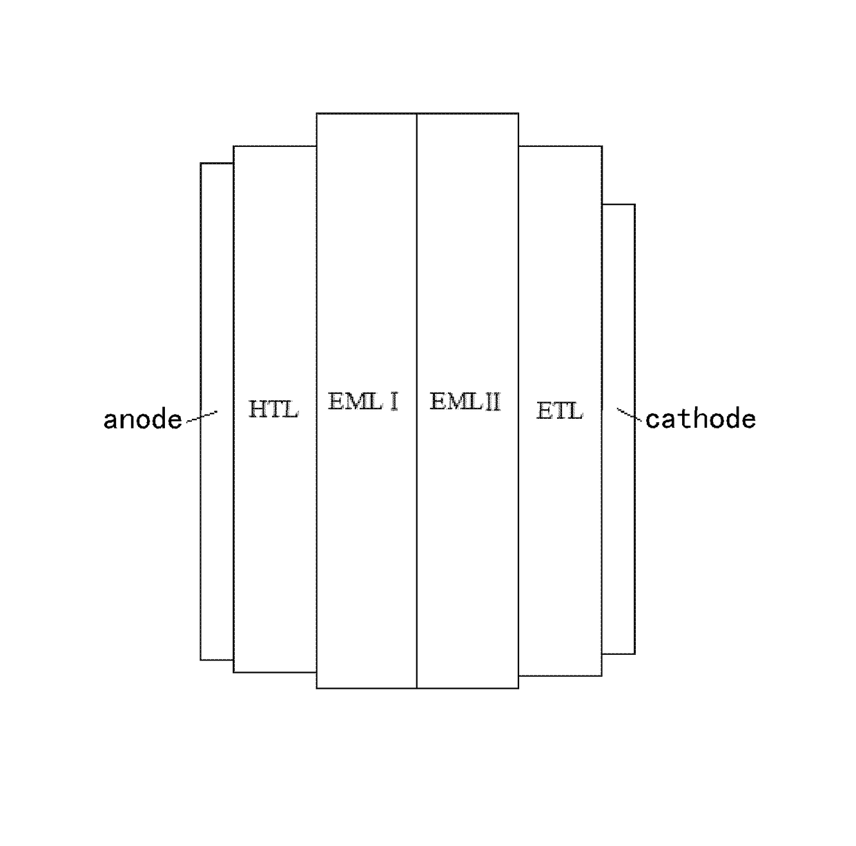
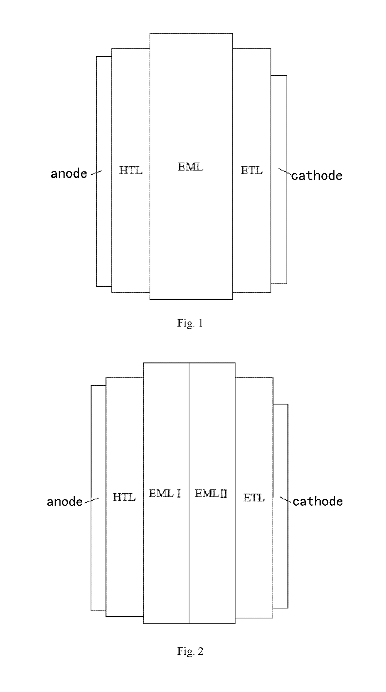
[0010]The existing substrate material for the light emitting layer is typically a hole-transport material or an electron-transport material. The embodiment of the present invention uses a same substrate material to prepare two light emitting layers, and makes a hole mobility of the first light emitting layer close to the anode equal to an electron mobility of the second light emitting layer close to the cathode; in this way, a balanced injection for electrons and holes is realized, and physical properties of these two light emitting layers are also matched with each other. In the embodiments of the present invention, two light emitting layers with the same substrate material are applied, which can realize a balanced injection for electrons and holes, thereby improving the efficiency and lifetime of the organic electroluminescent device.
[0021]The embodiment of the present invention uses a same substrate material to prepare two light emitting layers, and makes a hole mobility of the first light emitting layer close to the anode equal to an electron mobility of the second light emitting layer close to the cathode. In this way, a balanced injection for electrons and holes is realized, and physical properties of these two light emitting layers are also matched with each other. In the embodiments of the present invention, two light emitting layers with the same substrate material are applied, which can realize a balanced injection for electrons and holes, thereby improving the efficiency and lifetime of the organic electroluminescent device.
Problems solved by technology
However, there are some problems in the structure of top-emitting organic electroluminescent devices, such as low efficiency, high driving voltage, poor lifetime, viewing angle and so on.
However, it is difficult to obtain a light emitting material, of which the electron mobility and hole mobility are the same.
Due to the inconsistency between the electron-transport ability and hole-transport ability in the light emitting layer, the electrons and holes transported to the interface of the light emitting layer can not enter the light emitting layer and recombine with a same number, which is not beneficial for improving the efficiency and lifetime of the organic electroluminescent device.
Method used
Image
Click on the blue label to locate the original text in one second.
Reading with bidirectional positioning of images and text.
Examples
example 1
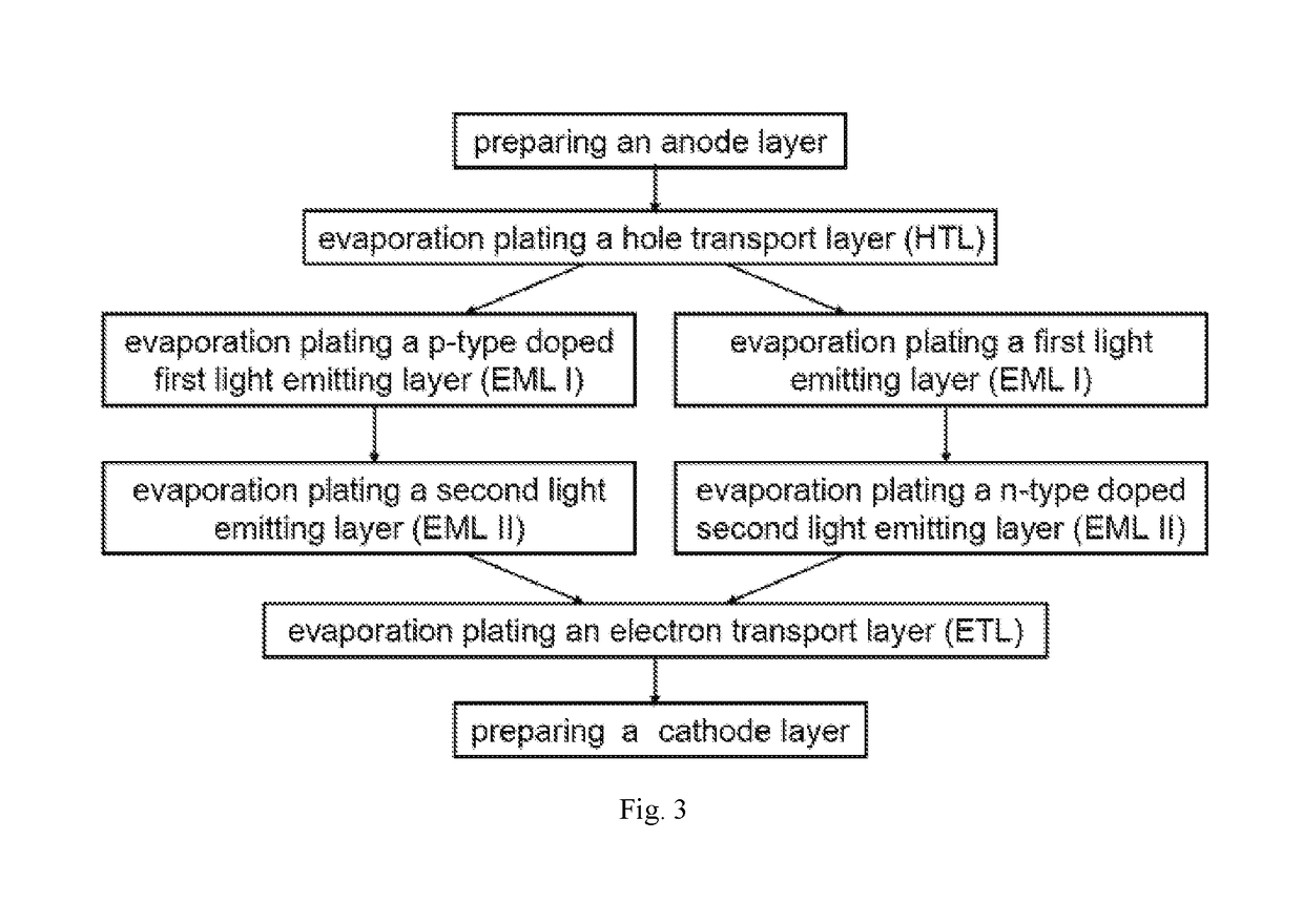
[0059]1) Sputtering an anode conductive film on a substrate. If the organic electroluminescent device is a top-emitting device, the anode layer can be made of a reflective material. If the organic electroluminescent device is a bottom-emitting device, the anode layer can be made of a transparent material; the material of the anode layer can be ITO (In2O3:SnO2), IZO (In2O3:ZnO), GITO (Ga0.08In0.28Sn0.64O3), or ZITO (Zn0.64In0.88Sn0.66O3);
[0060]2) After preparing the anode conductive film, preparing a hole transport layer (HTL) with vacuum evaporation process. Optionally, a material with a high hole mobility is used as the hole transport layer; a material of the hole transport layer can be N,N′-bis(1-naphthalenyl)-N,N′-diphenyl-1,1′-biphenyl-4,4′-diamine (NPB), triphenyl-diamine derivative (TPD), N,N′-bis(phenyl)-N,N′-bis(4′-(N,N-bis(phenylamino)-4-biphenyl)benzidine (TPTE), or 1,3,5-tris(N-3-methylphenyl-N-phenylamino)benzene (TDAB), etc.;
[0061]3) Preparing a first light emitting lay...
example 2
[0065]1) Sputtering an anode conductive film on a substrate. If the organic electroluminescent device is a top-emitting device, the anode layer can be made of a reflective material. If the organic electroluminescent device is a bottom-emitting device, the anode layer can be made of a transparent material. The material of the anode layer can be ITO (In2O3:SnO2), IZO (In2O3:ZnO), GITO (Ga0.08In0.28Sn0.64O3), or ZITO (Zn0.64In0.88Sn0.66O3);
[0066]2) After preparing the anode conductive film, preparing a hole transport layer (HTL) with vacuum evaporation process. Optionally, a material with a high hole mobility is used as the hole transport layer. A material of the hole transport layer can be N,N′-bis(1-naphthalenyl)-N,N′-diphenyl-1,1′-biphenyl-4,4′-diamine (NPB), triphenyl-diamine derivative (TPD), N,N′-bis(phenyl)-N,N′-bis(4′-(N,N-bis(phenylamino)-4-biphenyl)benzidine (TPTE), or 1,3,5-tris(N-3-methylphenyl-N-phenylamino)benzene (TDAB), etc.;
[0067]3) Preparing a first light emitting lay...
PUM
Property
Measurement
Unit
organic
aaaaa
aaaaa
hole mobility
aaaaa
aaaaa
electron mobility
aaaaa
aaaaa
Abstract
The embodiments of the present invention provide an organic electroluminescent device, a manufacturing method thereof and an electronic equipment. The organic electroluminescent device comprises: an anode layer, a hole transport layer, a first light emitting layer, a second light emitting layer, an electron transport layer, and a cathode layer stacked in sequence; wherein the first light emitting layer and the second light emitting layer comprise a same substrate material; the first light emitting layer and / or the second light emitting layer are doped such that a hole mobility of the first light emitting layer is equal to an electron mobility of the second light emitting layer. In the embodiments of the present invention, two light emitting layers with the same substrate material are applied, which can realize a balanced injection for electrons and holes, thereby improving the efficiency and lifetime of the organic electroluminescent device.
Description
RELATED APPLICATIONS[0001]The present application is the U.S. national phase entry of PCT / CN2015 / 087775, with an international filing date of Aug. 21, 2015, which claims the benefit of Chinese Patent Application No. 201510180124.7, filed on Apr. 16, 2015, the entire disclosures of which are incorporated herein by reference.FIELD OF THE INVENTION[0002]The present invention relates to the field of display technology, particularly to an organic electroluminescent device, a manufacturing method thereof and an electronic equipment.BACKGROUND OF THE INVENTION[0003]Organic electroluminescent devices (OLED) are highly valued in flat panel display and lighting fields due to the advantages of high brightness, color saturation, thin and light, flexible and so on. At present, a common organic electroluminescent device mainly comprises top-emitting device structure and bottom-emitting device structure. Compared with the bottom-emitting device structure, the top-emitting device structure has adva...
Claims
Application Information
Patent Timeline
Application Date:The date an application was filed.
Publication Date:The date a patent or application was officially published.
First Publication Date:The earliest publication date of a patent with the same application number.
Issue Date:Publication date of the patent grant document.
PCT Entry Date:The Entry date of PCT National Phase.
Estimated Expiry Date:The statutory expiry date of a patent right according to the Patent Law, and it is the longest term of protection that the patent right can achieve without the termination of the patent right due to other reasons(Term extension factor has been taken into account ).
Invalid Date:Actual expiry date is based on effective date or publication date of legal transaction data of invalid patent.

