Click on the blue label to locate the original text in one second.
Reading with bidirectional positioning of images and text.
Examples
Example
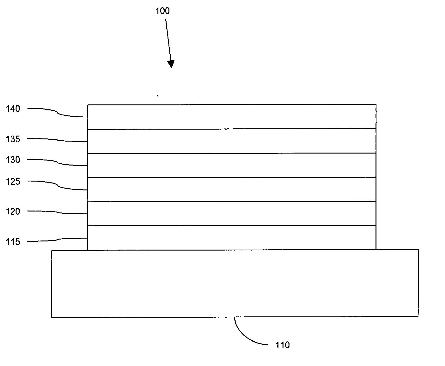
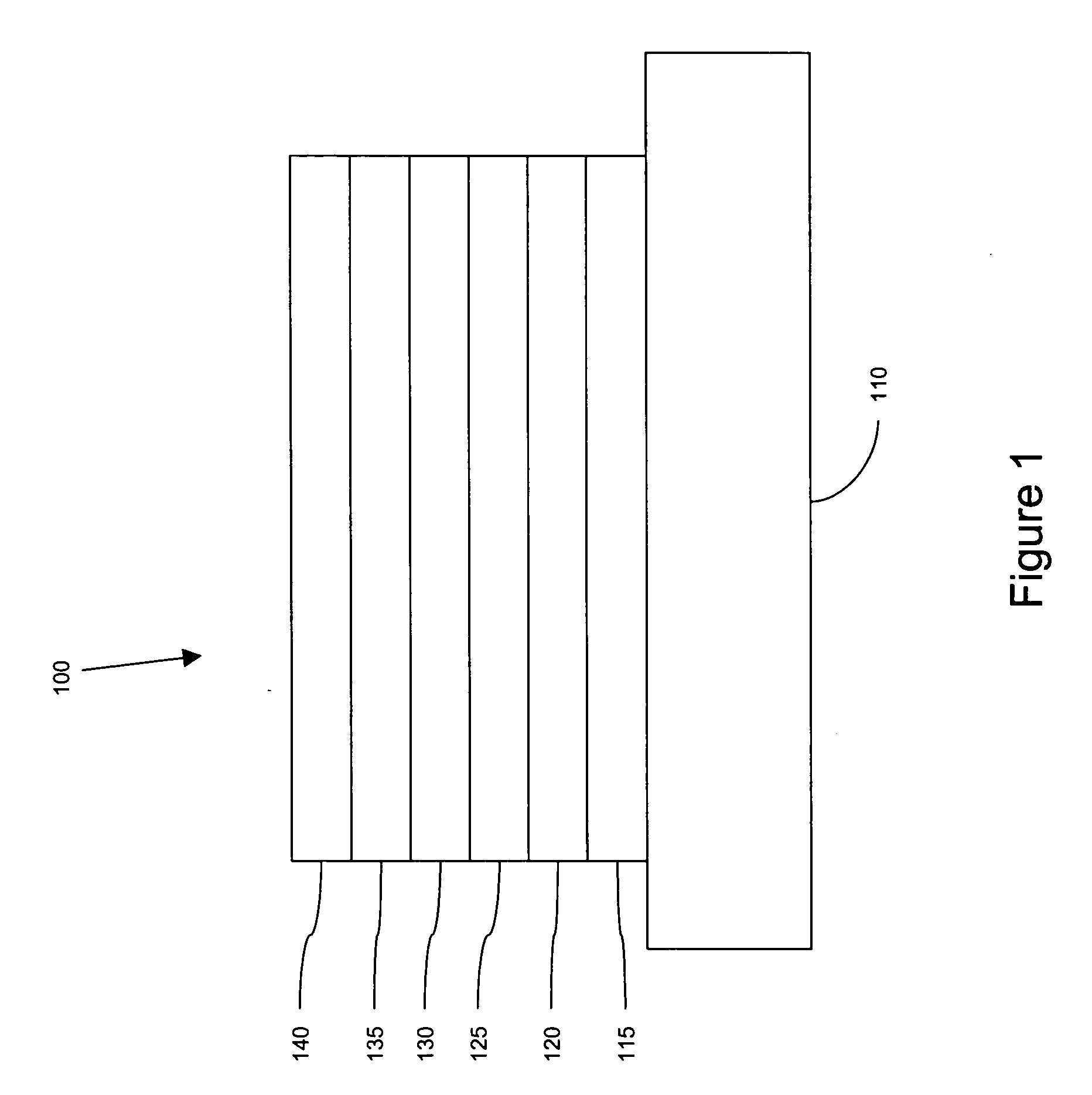
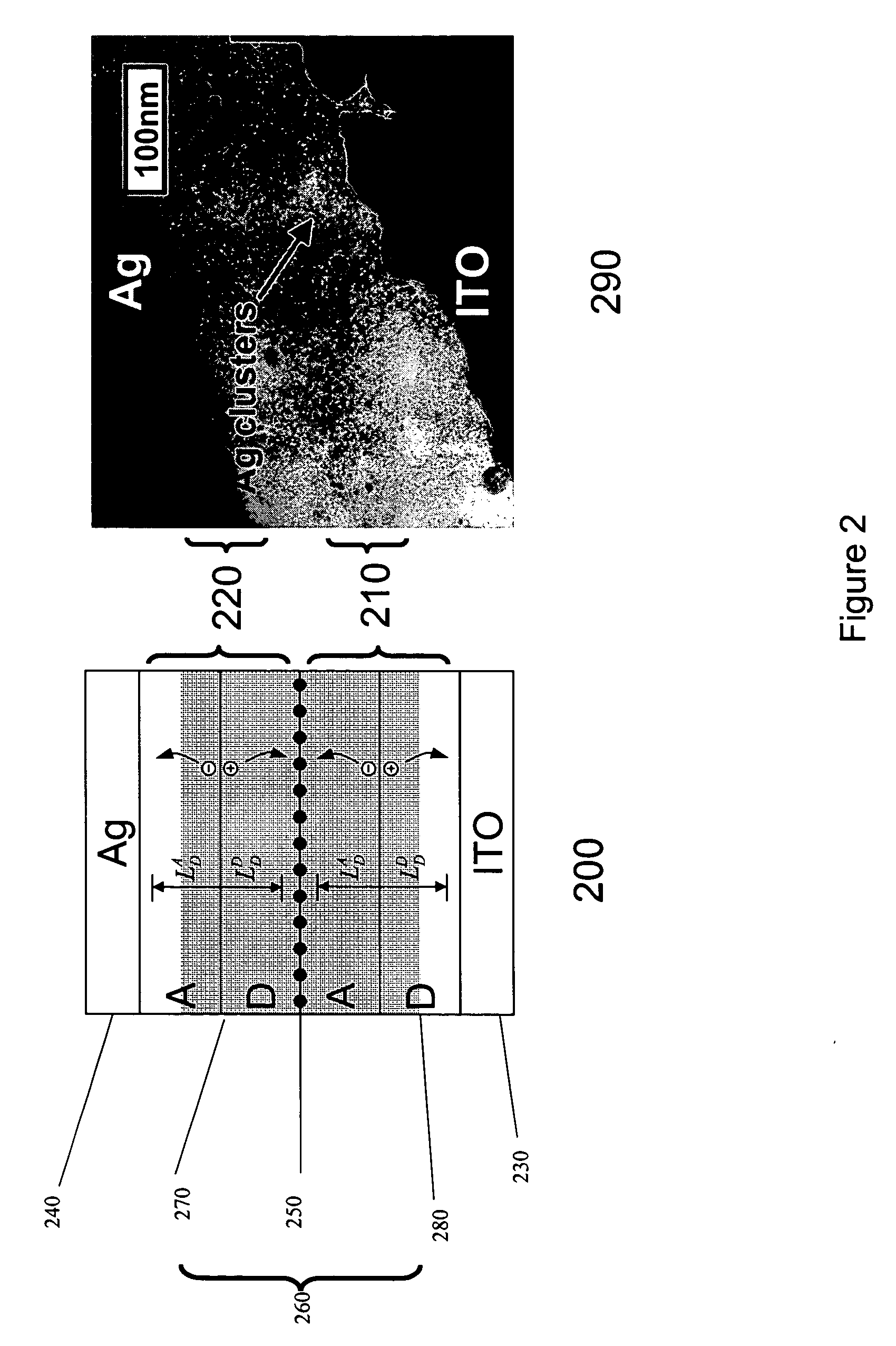
[0041] An organic photosensitive optoelectronic device is provided. Organic devices of embodiments of the present invention may be used, for example, to generate a usable electrical current from incident electromagnetic radiation (e.g., PV devices) or may be used to detect incident electromagnetic radiation. Embodiments of the present invention may comprise an anode, a cathode, and a photoactive region between the anode and the cathode. The photoactive region is the portion of the photosensitive device that absorbs electromagnetic radiation to generate excitons that may dissociate in order to generate an electrical current. Organic photosensitive optoelectronic devices may also include at least one transparent electrode to allow incident radiation to be absorbed by the device. Several PV device materials and configurations are described in U.S. Pat. Nos. 6,657,378, 6,580,027, and 6,352,777, which are incorporated herein by reference in their entirety.
[0042]FIG. 1 shows an organic p...
PUM
Abstract
The present invention generally relates to organic photosensitive optoelectronic devices. More specifically, it is directed to organic photosensitive optoelectronic devices having a photoactive organic region containing encapsulated nanoparticles that exhibit plasmon resonances. An enhancement of the incident optical field is achieved via surface plasmon polariton resonances. This enhancement increases the absorption of incident light, leading to a more efficient device.
Description
FIELD OF THE INVENTION [0001] The present invention generally relates to organic photosensitive optoelectronic devices. More specifically, it is directed to organic photosensitive optoelectronic devices having nanoparticles. BACKGROUND OF THE INVENTION [0002] Optoelectronic devices rely on the optical and electronic properties of materials to either produce or detect electromagnetic radiation electronically or to generate electricity from ambient electromagnetic radiation. [0003] Photosensitive optoelectronic devices convert electromagnetic radiation into electricity. Solar cells, also called photovoltaic (PV) devices, are a type of photosensitive optoelectronic device that is specifically used to generate electrical power. PV devices, which may generate electrical energy from light sources other than sunlight, can be used to drive power consuming loads to provide, for example, lighting, heating, or to power electronic circuitry or devices such as calculators, radios, computers or r...
Claims