[0009] An
advantage of some aspects of the invention is that it provides an electro-optical device capable of preventing a ghost from being generating without reducing a period for which a gray-scale signal is sampled to each data line, a
driving circuit of the same, and an electronic apparatus.
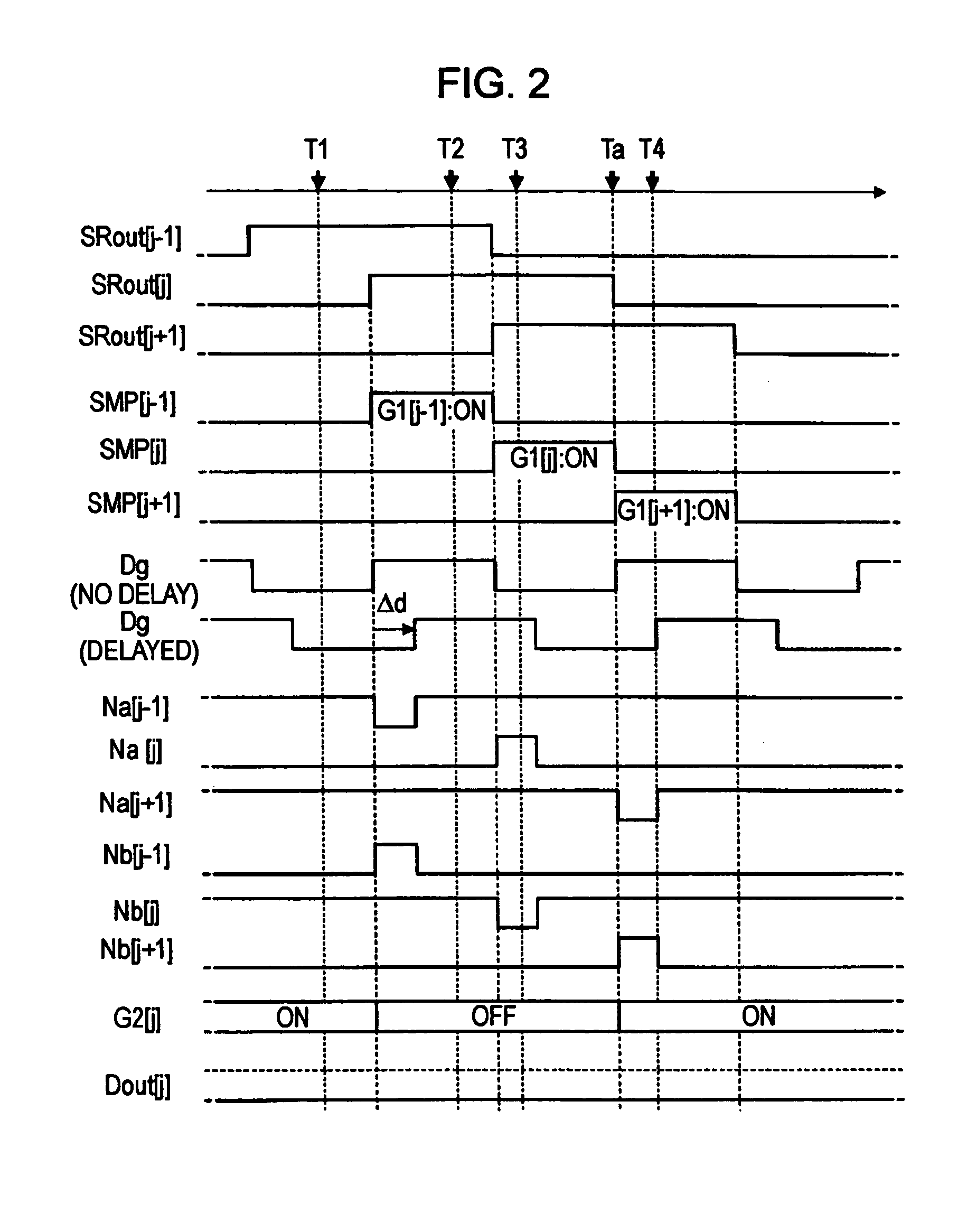
[0011] According to this aspect, since the second switching element enters an off state until the predetermined period passes from the time when the sampling starts by the first switching element, the supply of the gray-scale signal to the data line is stopped. Accordingly, if the amount of the delayed gray-scale signal with respect to the sampling period is within a range of a predetermined period, it is possible to prevent the voltage error of the data line from being generated due to the
delay. In addition, even when the second switching element is shifted from the on state to the off state for the predetermined period, a voltage of the output terminal of the second switching element (that is, a voltage applied to the data line or a voltage corresponding to the voltage) is held as a voltage right before the second switching element is shifted from the on state to the off state, by means of the storage
capacitor. Accordingly, the voltage according to the gray-scale signal can be applied to the data line with high precision, so that it is possible to prevent the ghost from being generated. The electro-optical element is an element whose optical characteristics such as the
transmittance or luminance vary in accordance with electrical operation. For example, the electro-optical element may be an inorganic EL
diode element, a light-emitting
diode element, or a
liquid crystal element as well as the
OLED element. Preferably, the storage
capacitor is a capacitor element of which one end is connected to the output terminal of the second switching element (for example, a capacitor C in preferred embodiment described below).
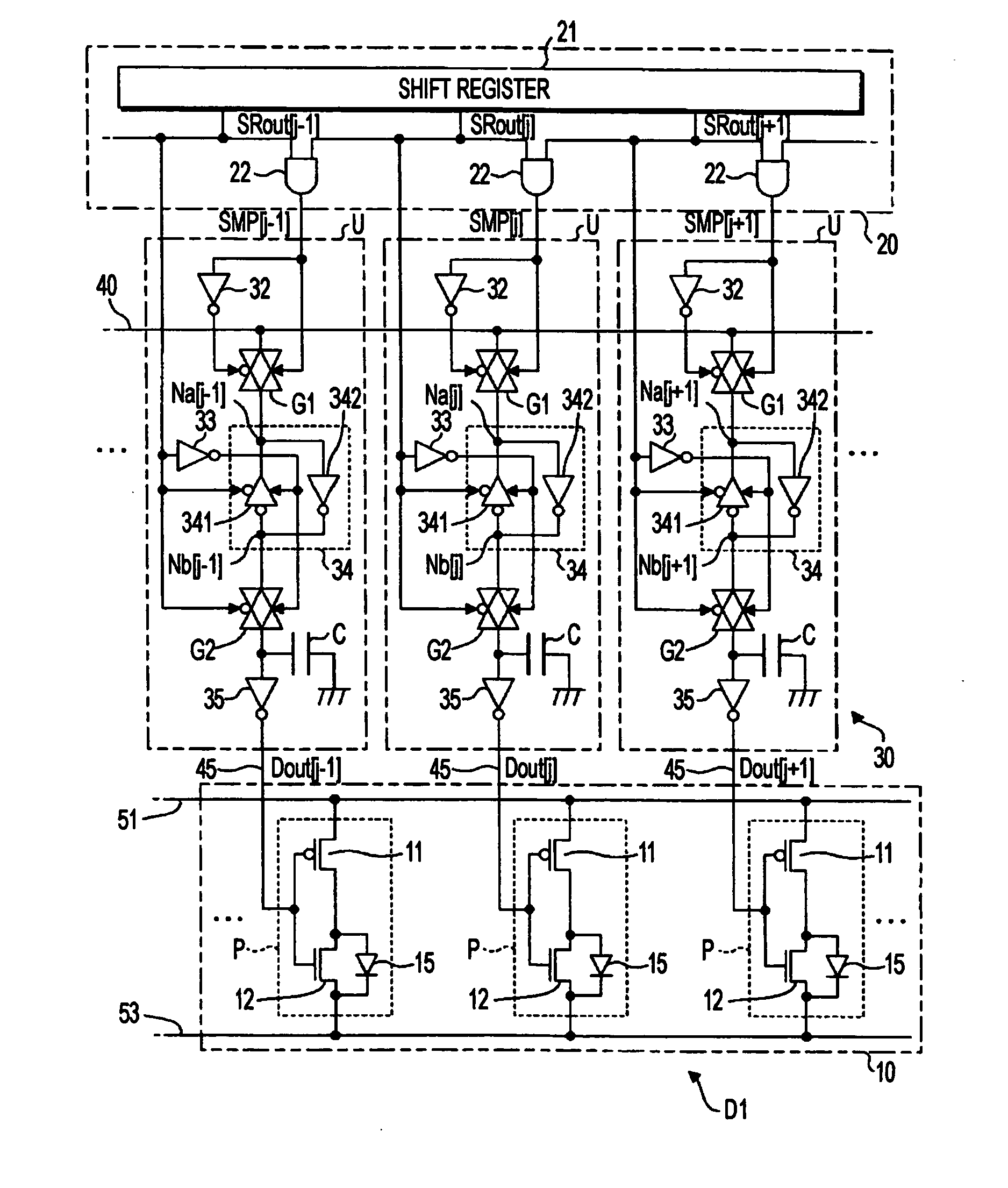
[0012] Preferably, the driving circuit further includes first and second potential supply lines each of which is supplied with an individual potential and a
smoothing capacitor that is inserted between the first potential supply line and the second potential supply line (for example, a capacitor C1 shown in FIG. 5 or 11). Preferably, the other end of the storage capacitor is connected to one end of the
smoothing capacitor. According to this aspect, it is possible to stabilize a voltage (and a voltage of the data line) held in the storage capacitor. Preferably, the driving circuit further includes an output buffer that is inserted between the second switching element and the data line (for example, an output buffer 35 shown in FIG. 5 and a clocked
inverter 38 shown in FIG. 11). Preferably, the first and second potential supply lines are wiring lines for supplying a power supply potential to the output buffer. According to this aspect, it is possible to simplify the structure of the wiring line of each unit circuit.
[0013] Preferably, the pulse output circuit has a
shift register that sequentially generates a plurality of pulse signals such that a period for which one pulse signal becomes an active level overlaps a period for which another pulse signal subsequent to the one pulse signal becomes an active level; and logical product circuits each of which outputs a logical product between one pulse signal and another pulse signal subsequent to the one pulse signal as a sampling pulse. Preferably, the second switching element of each unit circuit is controlled such that it is turned on or turned off in accordance with a pulse signal output from the
shift register. Preferably, each unit circuit has a logical sum circuit (for example, an OR circuit 36 shown in FIG. 7 or 13) that outputs a signal corresponding to logical sum between a sampling pulse input to the corresponding unit circuit and a sampling pulse input to a unit circuit located at a front stage of the corresponding unit circuit. The second switching element is controlled such that it is turned on or turned off in accordance with a signal output from the logical sum circuit. According to this aspect, it is possible to reduce the output load of the pulse output circuit and it is possible to simplify the structure of the wring line provided near the pulse output circuit.
[0016] Preferably, the electro-optical element is inserted between a first power supply line having a first potential (for example, an
anode-side power supply line 51 in preferred embodiments described below) and a second power supply line having a second potential different from the first potential (for example, a
cathode-side power supply line 53 in preferred embodiments described below). Further, the storage capacitor has a first capacitor element that has one end connected to an output terminal of the second switching element and has the other end connected to the first power supply line; and a second capacitor element that has one end connected to an output terminal of the second switching element and has the other end connected to the second power supply line. According to this aspect, even when the potential supplied to any one of the first power supply line and the second power supply line varies, it is possible to stably maintain the voltage of the data line.
[0017] In addition, an example of the storage capacitor is the capacitor element connected to the output terminal of the second switching element. However, it is not necessary that the storage capacitor is an element provided separately from the other elements. Preferably, the electro-optical device further includes a plurality of pixel circuits each of which has the above-mentioned electro-optical element, and each of the plurality of pixel circuits has a
transistor that controls a voltage applied to the electro-optical element in accordance with a voltage applied to a gate
electrode through the data line. Preferably, the storage capacitor is a gate capacitor of the
transistor (a gate capacitor Cg shown in FIGS. 10 to 14). According to this aspect, it is possible to reduce a size of the circuit as compared with a structure in which the storage capacitor is a separated element.

