Semiconductor light emitting device

a technology of light-emitting devices and semiconductors, which is applied in the manufacture of semiconductor/solid-state devices, semiconductor devices, and electrical equipment, etc., can solve the problems of small trouble, short-circuits, and wiring breakage, and achieve high reliability

Inactive Publication Date: 2006-11-23
ROHM CO LTD
View PDF3 Cites 20 Cited by
  • Summary
  • Abstract
  • Description
  • Claims
  • Application Information

AI Technical Summary

Benefits of technology

[0017] As a result, problems such that the short-circuit occurrence between the light emitting units or a break-circuit of the wiring hardly arise and a semiconductor light emitting device with high reliability can be obtained. In addition, in case that one of the twofold separating grooves is formed so as to work for a block of the plurality of adjacent light emitting units with an aspect of an e

Problems solved by technology

And, as a wiring film is formed on the separating groove, when a width of the separating groove is wide, a problem of a break in wiring may arise.
As a result, the short-circuit occasionally arises due to the contaminations embedded in the separating groove, even if light emitting units are separated by forming the separating groves.
Under the above-described condition, in case of the short-circuit between two vertically adjacent light emitting units as shown in FIG. 5, as only one

Method used


Image

  • Semiconductor light emitting device
  • Semiconductor light emitting device
  • Semiconductor light emitting device

Examples


Embodiment Construction

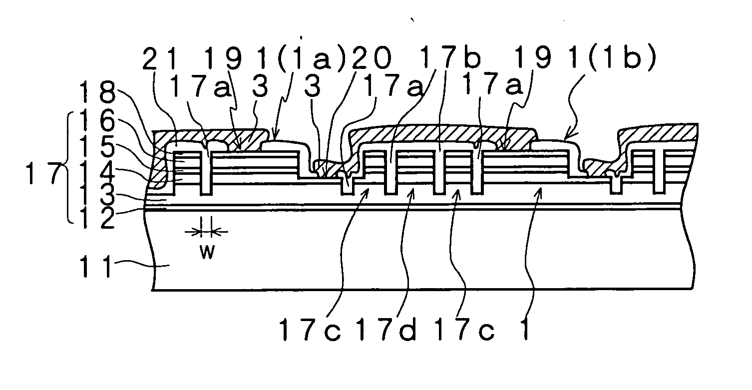
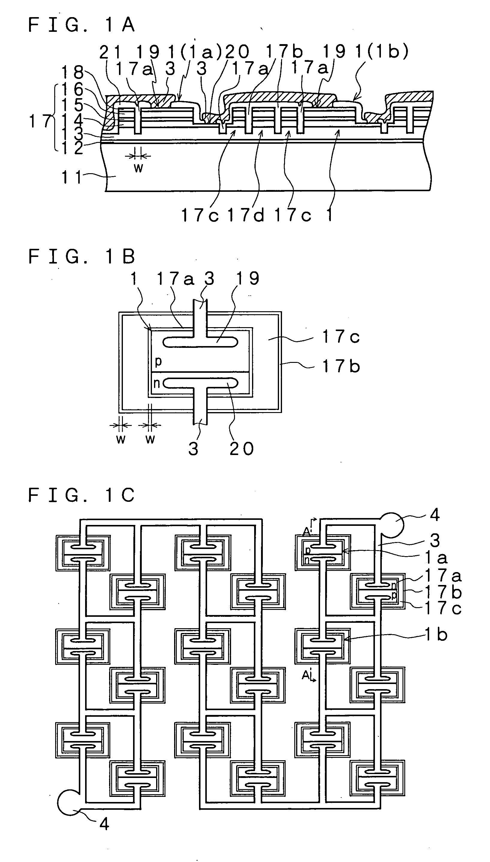
[0024] An explanation will be given below of a semiconductor light emitting device according to the present invention in reference to the drawings. FIGS. 1A through 1C are figures showing one embodiment of the semiconductor light emitting device according to the present invention, FIG. 1A is an explanatory figure showing a cross-sectional view (a cross-sectional view of A-A in FIG. 1C), FIG. 1B is an explanatory figure showing a plane view of one light emitting unit, and FIG. 1C is a explanatory figure showing a plane view of the whole example.

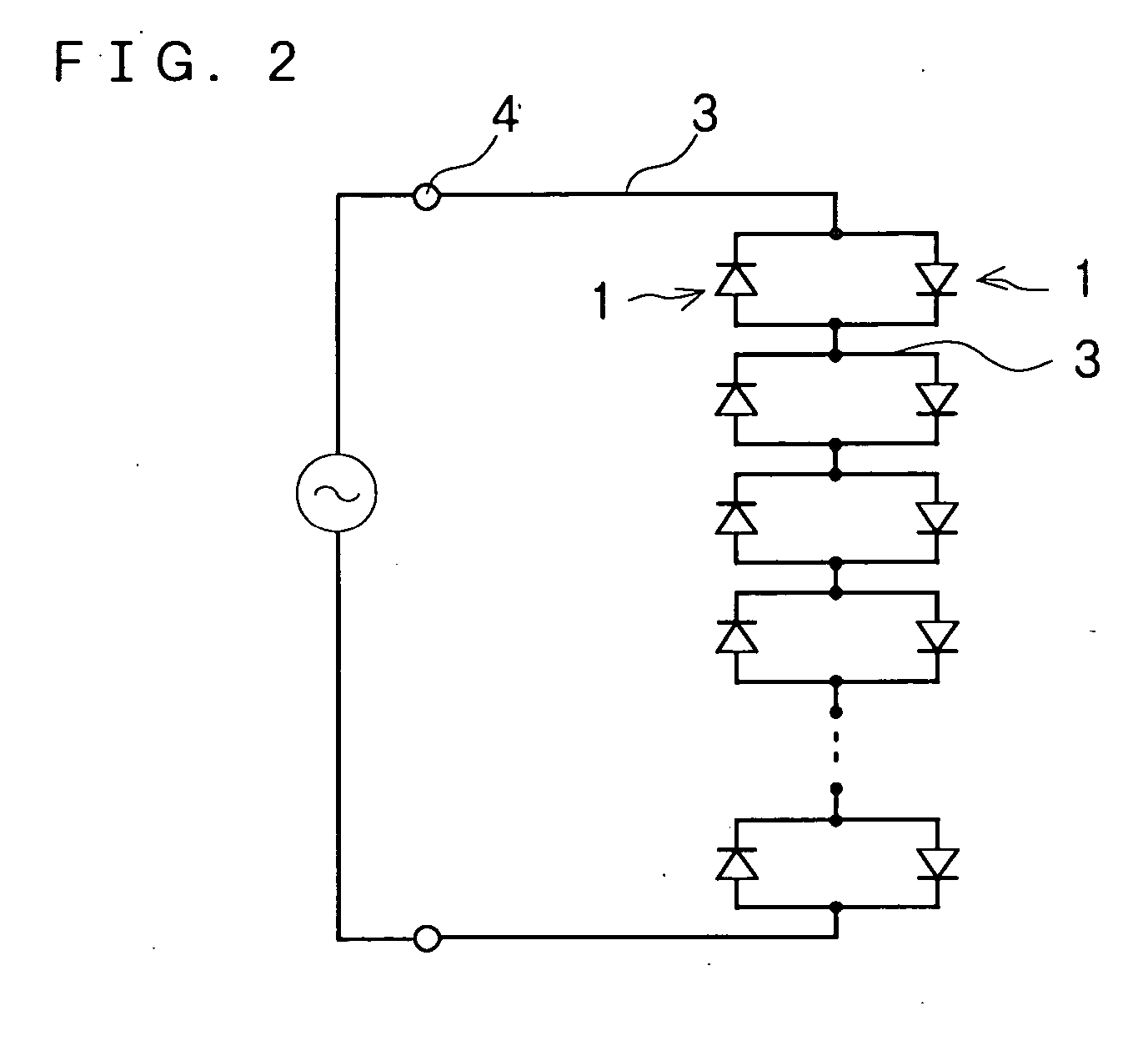
[0025] As shown in FIGS. 1A through 1C, the semiconductor light emitting device according to the present invention includes a semiconductor lamination portion 17 formed on a substrate 1 by laminating semiconductor layers so as to form a light emitting layer. The semiconductor lamination portion 17 is electrically separated into a plurality of light emitting units 1 (1a, 1b). Each of the plurality of light emitting units has a pair of electric...


PUM


Abstract

A semiconductor lamination portion is formed on a substrate by laminating semiconductor layers so as to form a light emitting layer, and a plurality of light emitting units are formed by separating the semiconductor lamination portion electrically into a plurality of units. Each of the units has a pair of electric connecting portions which are connected to a pair of conductivity type layers and they are connected to each other with a wiring film. Each of the plurality of the light emitting units is separated electrically by dividing the conductivity type layers of the semiconductor lamination portion with at least twofold separating grooves (a first separating groove and a second separating groove). As a consequence, a semiconductor light emitting device with a high luminance and being formed in a monolithic type having a plurality of light emitting units can be obtained to solve a problem of a short-circuit occurrence between the light emitting units while keeping high reliability of wiring or the like.

Description

FIELD OF THE INVENTION [0001] The present invention relates to a semiconductor light emitting device in which a plurality of light emitting units are formed on a substrate and connected in series and / or parallel, and which can be used for light sources in place of incandescent lamps or fluorescent lamps used with commercial AC power sources of, for example, 100 V, or be used for signs or car-lights. More particularly, the present invention relates to a semiconductor light emitting device which has a structure with high reliability such that a problem of stopping operation of the light emitting device caused by a fault such as a short-circuit between the light emitting units hardly arises. BACKGROUND OF THE INVENTION [0002] Being accompanied with developing blue light emitting diodes (LEDs), LEDs are lately used for light sources of displays or traffic signals and furthermore become to be used in place of incandescent lamps or fluorescent lamps. As it is preferable that LEDs can be o...

Claims


Application Information

Patent Timeline
IPC IPC(8): H01L33/00H01L33/06H01L33/08H01L33/32H01L33/42H01L33/50
CPCH01L27/156
Inventor SHAKUDA, YUKIO
Owner ROHM CO LTD
Why Eureka
Try Eureka