
Etchant composition, and method of fabricating metal pattern and thin film transistor array panel using the same
- Summary
- Abstract
- Description
- Claims
- Application Information
AI Technical Summary
Benefits of technology
Problems solved by technology
Method used
Image

Examples
examples
[0068]A display panel with metal wiring layers containing copper or a copper alloy was fabricated.
[0069]A substrate based on a glass material with a size of about 300× about 400 mm was prepared, and metal layers containing copper or a copper alloy were deposited onto the substrate as gate and data lines. A photoresist pattern was formed on the metal layers.
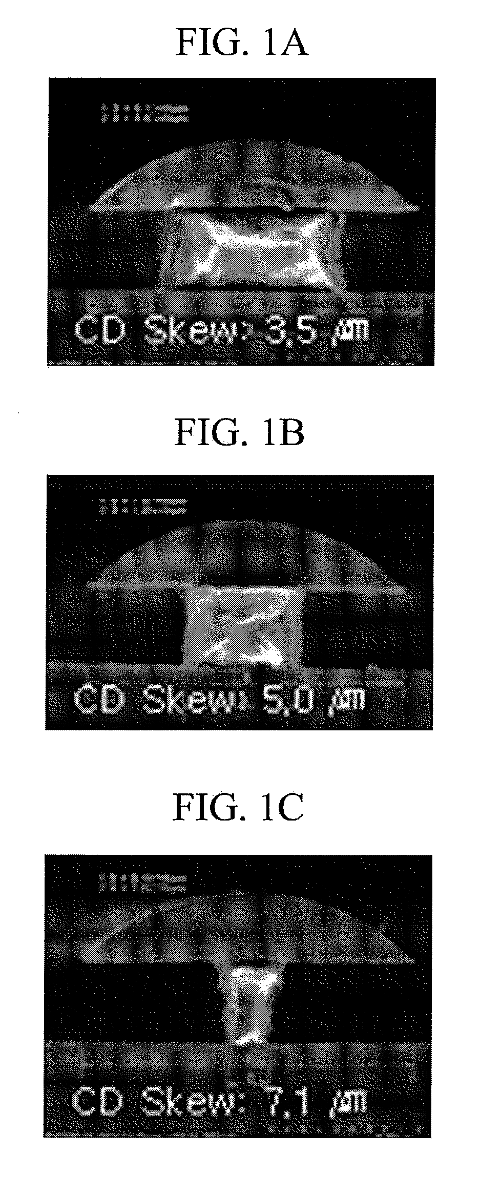
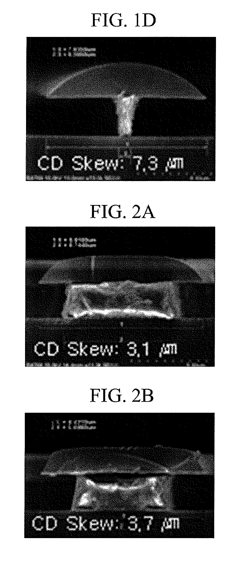
[0070]An etchant composition of about 180 kg containing phosphoric acid (H3PO4), nitric acid (HNO3), acetic acid (CH3COOH), glycolic acid, sodium dihydrogen phosphate, iminodiacetic acid, and water in accordance with the composition ratios listed in Table 1 was prepared. The etchant composition was put into experimental spray etching equipment (manufactured by K. C Tech Company, model ETCHER(TFT)), and the etching process was conducted at about 30° C., about 33° C., and about 35° C. The total etch time was established such that the time detected by an end point detector (EPD) was added by the amounts of about 50%, about 70%, about...
PUM
| Property | Measurement | Unit |
|---|---|---|
| Fraction | aaaaa | aaaaa |
| Fraction | aaaaa | aaaaa |
| Fraction | aaaaa | aaaaa |
Abstract
Description
Claims
Application Information