Check patentability & draft patents in minutes with Patsnap Eureka AI!
Substrate processing apparatus
What is Al technical title?
Al technical title is built by PatSnap Al team. It summarizes the technical point description of the patent document.
a processing apparatus and substrate technology, applied in the field of substrate processing apparatuses, can solve the problems of defective dimension, defective shape of exposure pattern, and inability to make a resist pattern finer than
Inactive Publication Date: 2010-06-03
SCREEN SEMICON SOLUTIONS CO LTD
View PDF80 Cites 21 Cited by
Summary
Abstract
Description
Claims
Application Information
AI Technical Summary
This helps you quickly interpret patents by identifying the three key elements:
Problems solved by technology
Method used
Benefits of technology
Benefits of technology
[0013]It is an object of the invention to provide a substrate processing apparatus capable of preventing a component of a photosensitive material on a substrate from being eluted in a liquid in an exposure device.
Problems solved by technology
With such conventional exposure devices, however, the line width of an exposure pattern is determined by the wavelength of the light source of an exposure device, thus making it impossible to make a resist pattern finer than that.
The resist component eluted in the liquid remains on a surface of the substrate, which may become the cause of a defect.
This may cause a defective dimension and a defective shape of the exposure pattern.
Method used
Image
Click on the blue label to locate the original text in one second.
Reading with bidirectional positioning of images and text.
Examples
Embodiment Construction
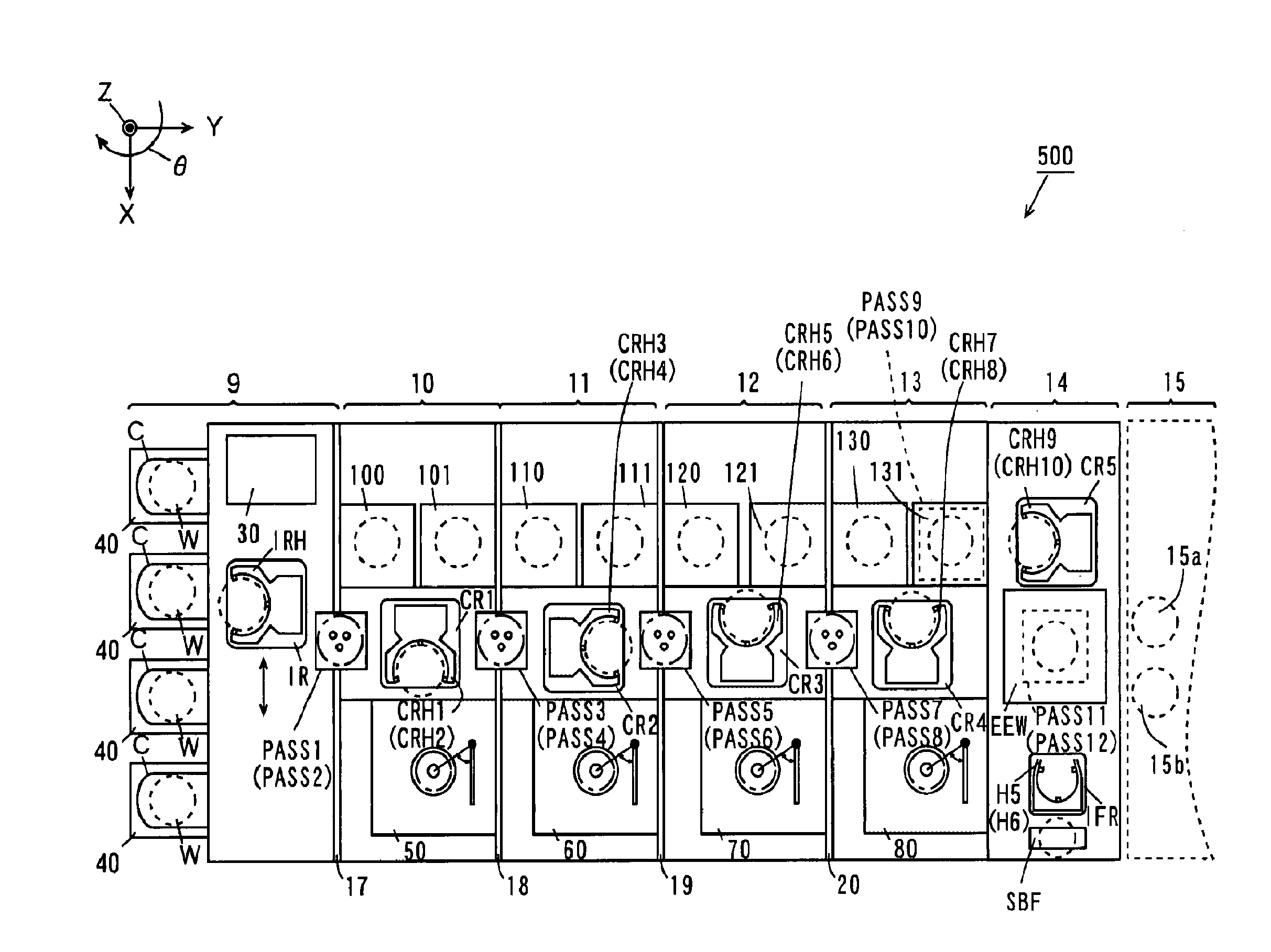
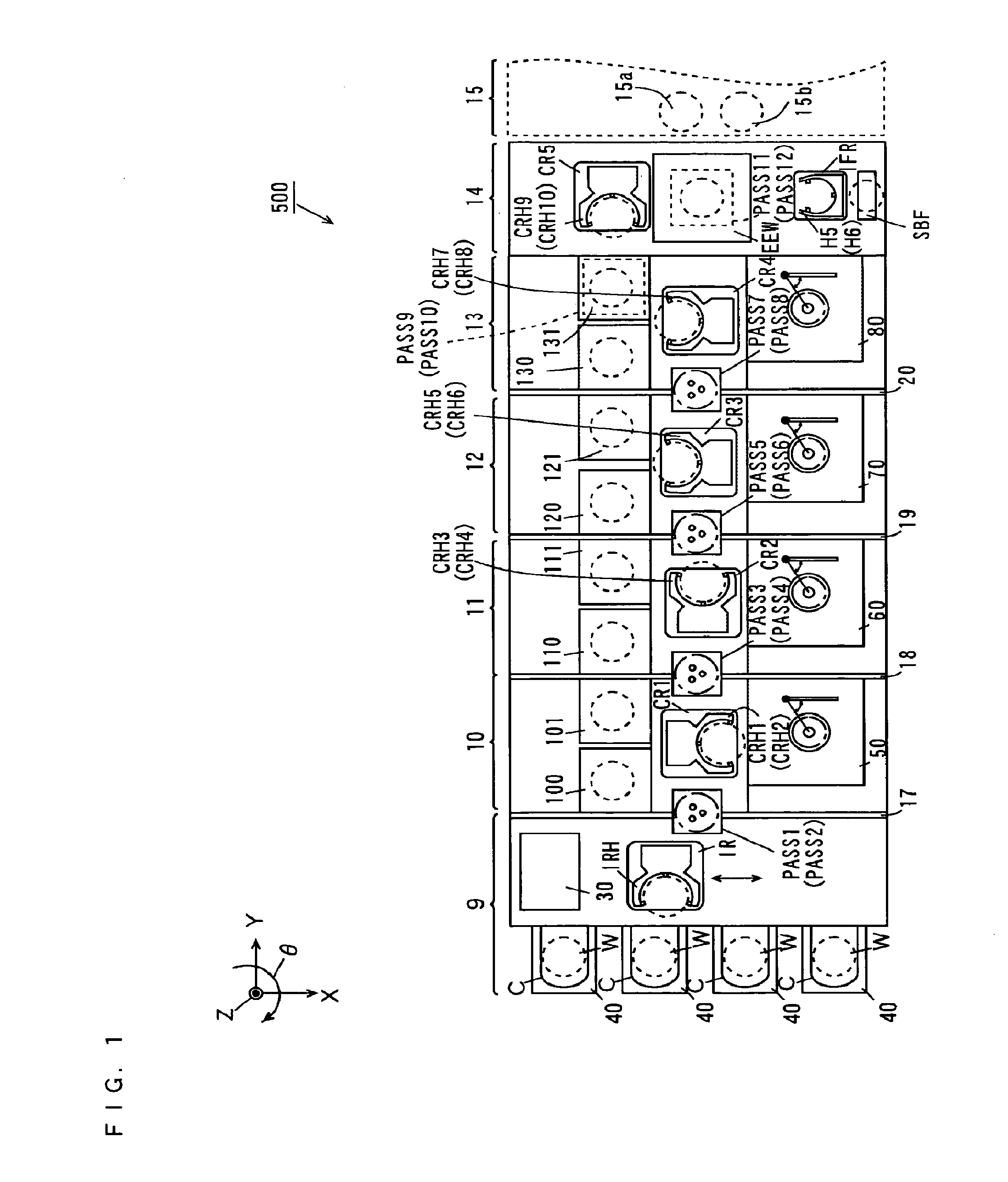
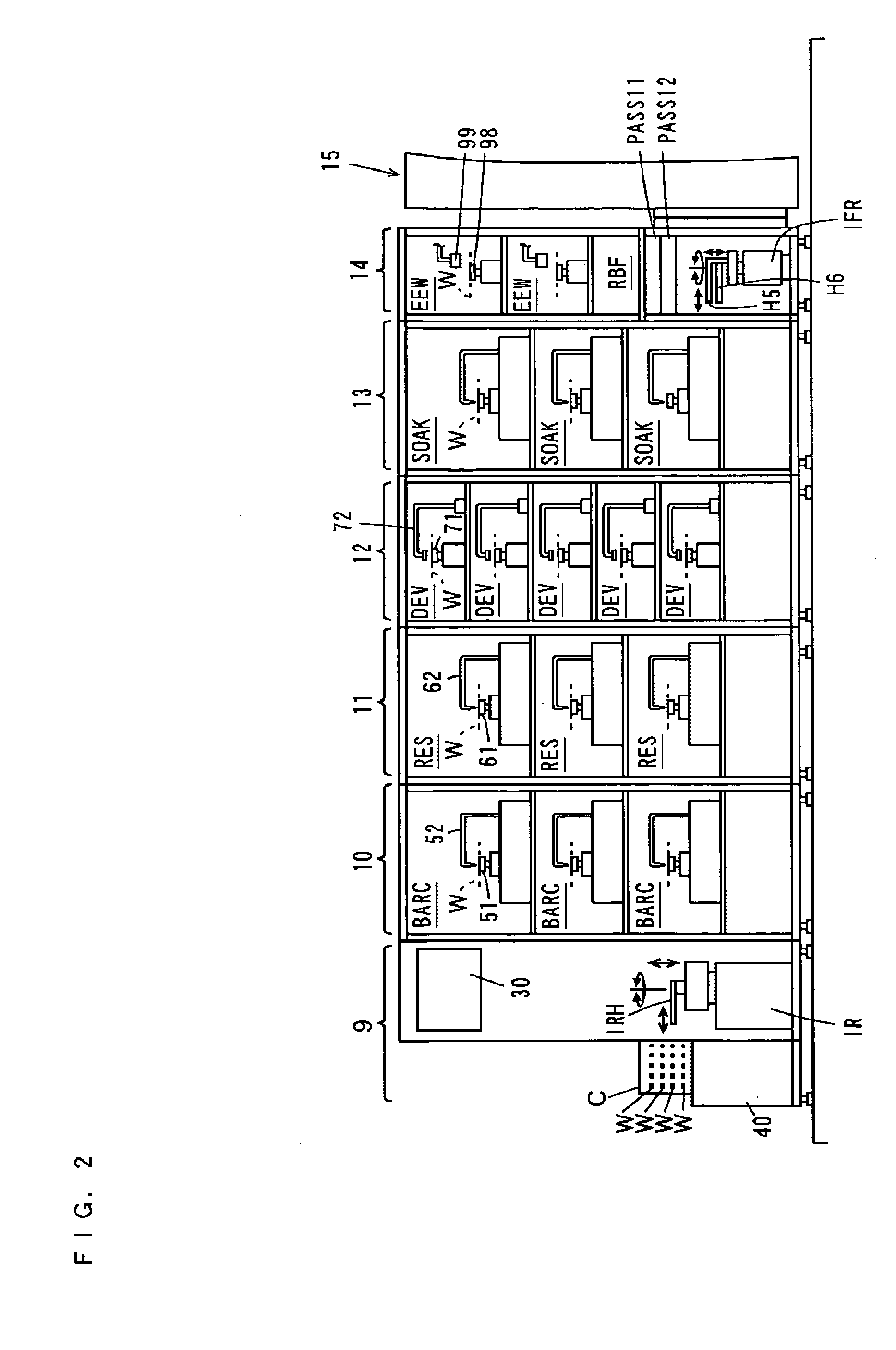
[0080]A substrate processing apparatus according to an embodiment of the invention will be described with reference to the drawings. A substrate as used in the specification includes a semiconductor substrate, a substrate for a liquid crystal display, a substrate for a plasma display, a glass substrate for a photomask, a substrate for an optical disk, a substrate for a magnetic disk, a substrate for a magneto-optical disk, and a substrate for a photomask.
[0081]FIG. 1 is a plan view of the semiconductor laser apparatus according to the embodiment of the invention.
[0082]Each of FIG. 1 and the subsequent drawings is accompanied by the arrows that indicate
[0083]X, Y, and Z directions perpendicular to one another for clarification of positions. The X and Y directions are perpendicular to each other in a horizontal plane, and the Z direction corresponds to the vertical direction. In each of the directions, the direction toward an arrow is defined as + direction, and the opposite direction...
PUM
Abstract
A method of processing a substrate in a substrate processing apparatus that is arranged adjacent to an exposure device and includes first, second and third processing units, includes forming a photosensitive film on the substrate by said first processing unit before exposure processing by said exposure device and applying washing processing to the substrate by supplying a washing liquid to the substrate in said second processing unit after the formation of said photosensitive film and before the exposure processing. The method also includes applying drying processing to the substrate in said second processing unit after the washing processing by said second processing unit and before the exposure processing and applying development processing to the substrate by said third processing unit after the exposure processing. Applying the drying processing to the substrate includes the step of supplying an inert gas onto the substrate, to which the washing liquid is supplied.
Description
CROSS-REFERENCES TO RELATED APPLICATIONS[0001]This application is a division of U.S. patent application Ser. No. 11 / 295,216, filed Dec. 6, 2005, which claims priority to Japanese Patent Application No. 2004-353120, filed Dec. 6, 2004, Japanese Patent Application 2005-095783, filed Mar. 29, 2005, and Japanese Patent Application No. 2005-267331, filed on Sep. 14, 2005. The disclosures of 11 / 295,216, JP 2004-353120, 2005-095783, and JP 2005-267331 are hereby incorporated by reference in their entirety for all purposes.[0002]The present application is related to the following four applications filed Dec. 6, 2005, and commonly owned: 1) U.S. patent application Ser. No. 11 / 294,877, entitled “SUBSTRATE PROCESSING APPARATUS AND SUBSTRATE PROCESSING METHOD,” 2) U.S. patent application Ser. No. 11 / 295,257, entitled “SUBSTRATE PROCESSING APPARATUS,” 3) U.S. patent application Ser. No. 11 / 294,727, entitled “SUBSTRATE PROCESSING APPARATUS,” and 4) U.S. patent application Ser. No. 11 / 295,240, ent...
Claims
Application Information
Patent Timeline
Application Date:The date an application was filed.
Publication Date:The date a patent or application was officially published.
First Publication Date:The earliest publication date of a patent with the same application number.
Issue Date:Publication date of the patent grant document.
PCT Entry Date:The Entry date of PCT National Phase.
Estimated Expiry Date:The statutory expiry date of a patent right according to the Patent Law, and it is the longest term of protection that the patent right can achieve without the termination of the patent right due to other reasons(Term extension factor has been taken into account ).
Invalid Date:Actual expiry date is based on effective date or publication date of legal transaction data of invalid patent.
Patent Type & Authority Applications(United States)
