Capacitive Touch Panel

a touch panel and capacitive technology, applied in the direction of electronic switching, instruments, pulse techniques, etc., can solve the problems of high manufacturing costs, and achieve the effect of low manufacturing costs and simple single layer structur

Inactive Publication Date: 2010-07-01
ACROSENSE TECH
View PDF5 Cites 95 Cited by
  • Summary
  • Abstract
  • Description
  • Claims
  • Application Information

AI Technical Summary

Benefits of technology

[0007]Therefore, the object of the present invention is to provide a capacitive touch panel that has a simple single layer structure on a surface of a substrate and thus attains low manufacturing costs.

Problems solved by technology

Moreover, the aforementioned two conventional capacitive touch panels are disadvantageous in that they have complicated layer structures and require complicated manufacturing processes, which results in high manufacturing costs.

Method used


Image

  • Capacitive Touch Panel
  • Capacitive Touch Panel
  • Capacitive Touch Panel

Examples


Embodiment Construction

[0021]Before the present invention is described in greater detail with reference to the accompanying preferred embodiments, it should be noted herein that like elements are denoted by the same reference numerals throughout the disclosure.

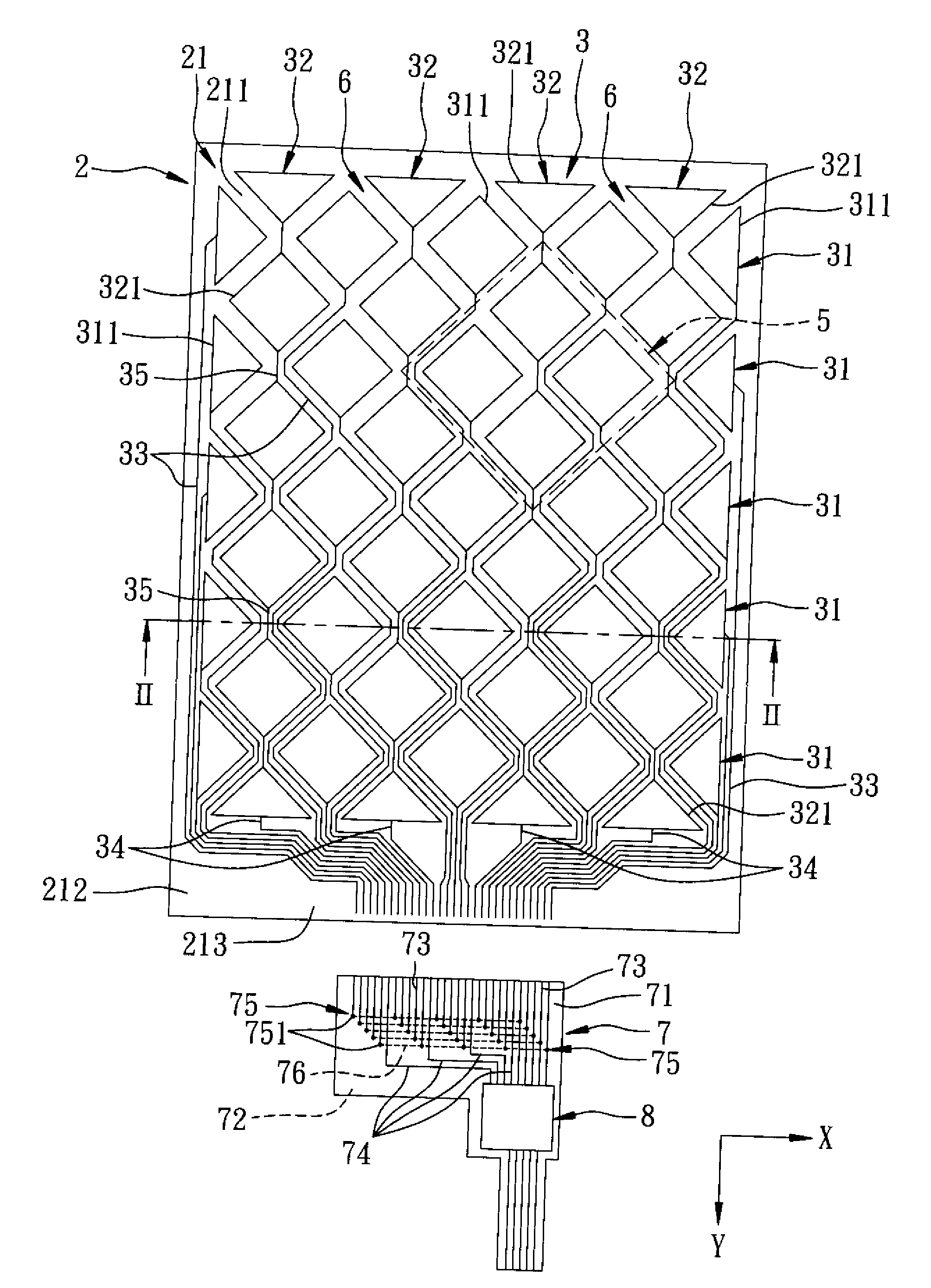
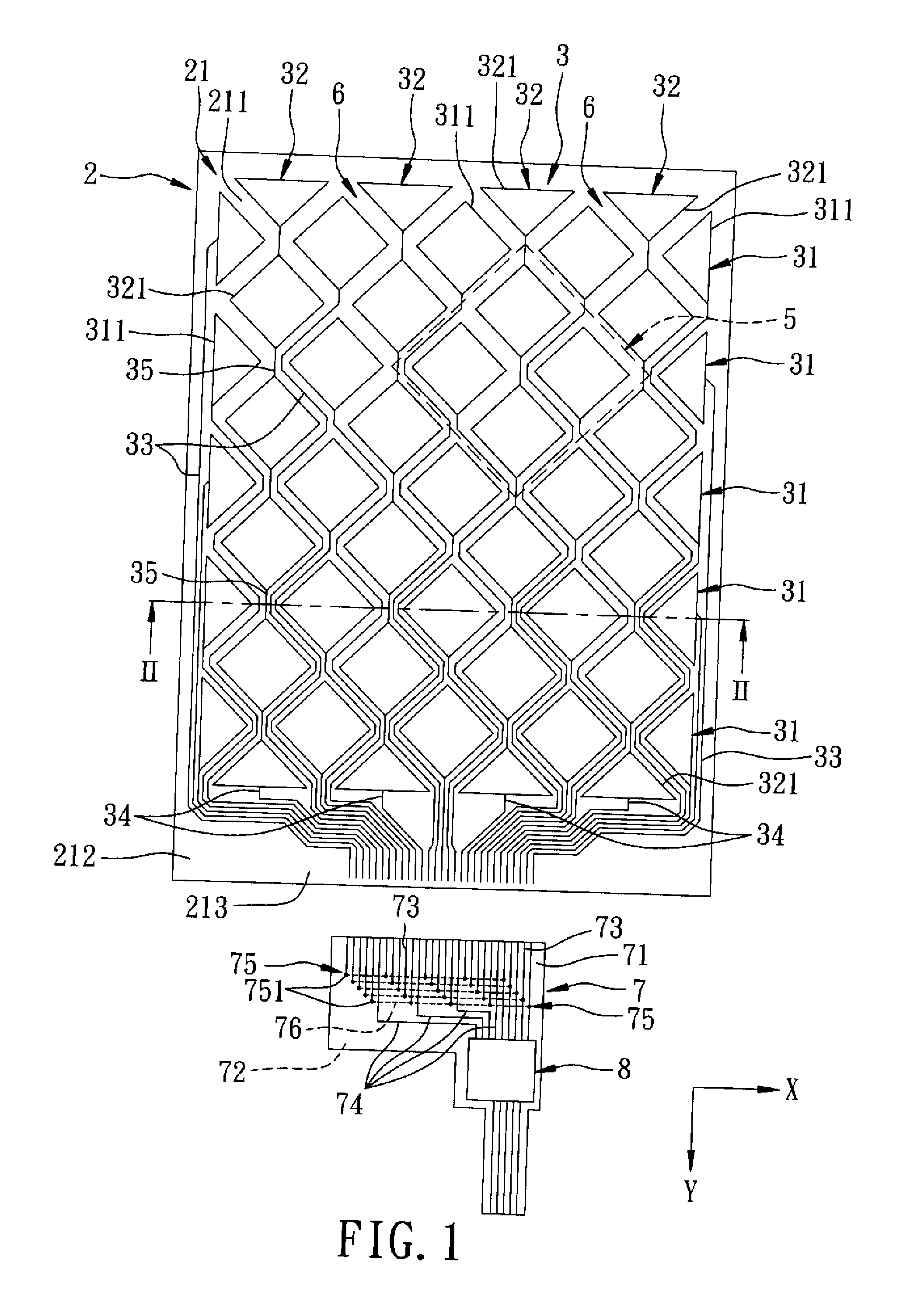
[0022]FIGS. 1 to 3 illustrate the first preferred embodiment of a capacitive touch panel according to this invention. The capacitive touch panel is connected to a controller 8, and includes a substrate 2, a patterned conductive layer 3, and a connector 7.

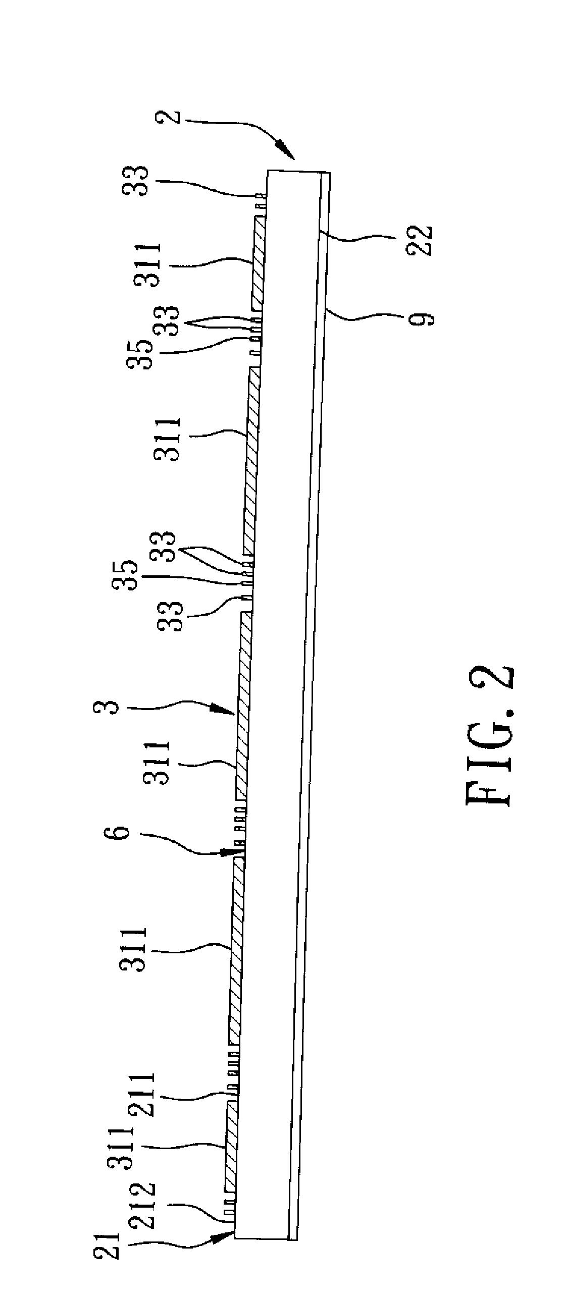
[0023]The substrate 2 has a pattern-forming surface 21 that is divided into an electrode-forming region 211 and a peripheral region 212. The peripheral region 212 surrounds the electrode-forming region 211, and has a bonding area 213 adjacent to a bottom side of the electrode-forming region 211.

[0024]The patterned conductive layer 3 is formed on the pattern-forming surface 21, and includes a plurality of first electrode units 31 formed on the electrode-forming region 211 and aligned in a first direc...


PUM


Abstract

A capacitive touch panel includes a substrate and a patterned conductive layer formed on the substrate. The patterned conductive layer includes a plurality of first electrode units, a plurality of second electrode units, a plurality of spaced apart first conductive lines, and a plurality of spaced apart second conductive lines. The first electrode units are capacitively coupled to the second electrode units so as to form a plurality of two dimensionally arranged capacitive sensing units. Each of the first electrode units includes a plurality of first electrodes. Each of the first conductive lines is connected to and extends from at least one of the first electrodes of a respective one of the first electrode units. The second conductive lines extend respectively from the second electrode units, and do not cross the first conductive lines.

Description

CROSS-REFERENCE TO RELATED APPLICATION[0001]This application claims priority of Taiwanese Application No. 097151643, filed on Dec. 31, 2008, the contents of which are incorporated by reference herein.BACKGROUND OF THE INVENTION[0002]1. Field of the Invention[0003]This invention relates to a capacitive touch panel, more particularly to a capacitive touch panel including a patterned conductive layer having two dimensionally arranged first and second electrodes and first and second conductive lines which are grown directly on the same surface of a substrate.[0004]2. Description of the Related Art[0005]Taiwanese Application No. 096115152 discloses a conventional capacitive touch panel that includes a substrate, alternately disposed first and second electrodes formed on the substrate, first conductive lines, second conductive lines, and insulator pads. The first electrodes are arranged into parallel columns. The second electrodes are arranged into parallel rows. Each of the first conduct...

Claims


Application Information

Patent Timeline
Patent Type & Authority Applications(United States)
IPC IPC(8): H03K17/975
CPCG06F3/0416G06F3/044H03K17/9622H03K2217/960755G06F3/04164G06F3/0443G06F3/0446
Inventor TANG, TUNG-YANGCHANG, HUNG-JUNG
Owner ACROSENSE TECH
Why Eureka
Try Eureka