

Low phase noise amplifier circuit
a low-phase noise, amplifier circuit technology, applied in the direction of dc-amplifiers with dc-coupled stages, amplifiers with semiconductor devices/discharge tubes, different amplifiers, etc., can solve the problems of signal phase noise degradation, generally significant phase noise degradation, and no provision for avoiding phase noise degradation. , to achieve the effect of convenient operation
- Summary
- Abstract
- Description
- Claims
- Application Information
AI Technical Summary
Benefits of technology
Problems solved by technology
Method used
Image

Examples
Embodiment Construction
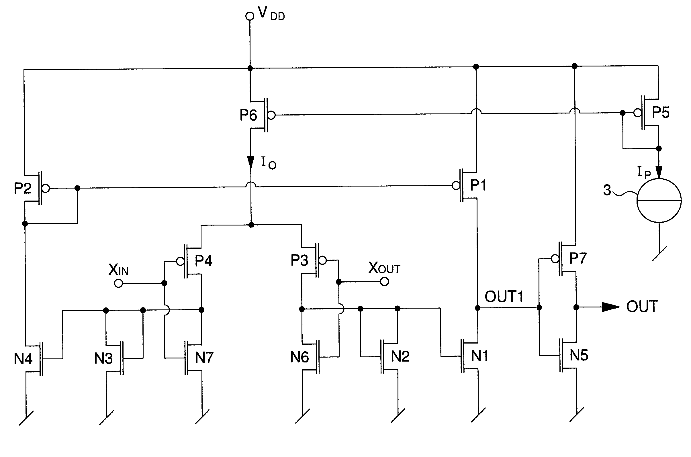
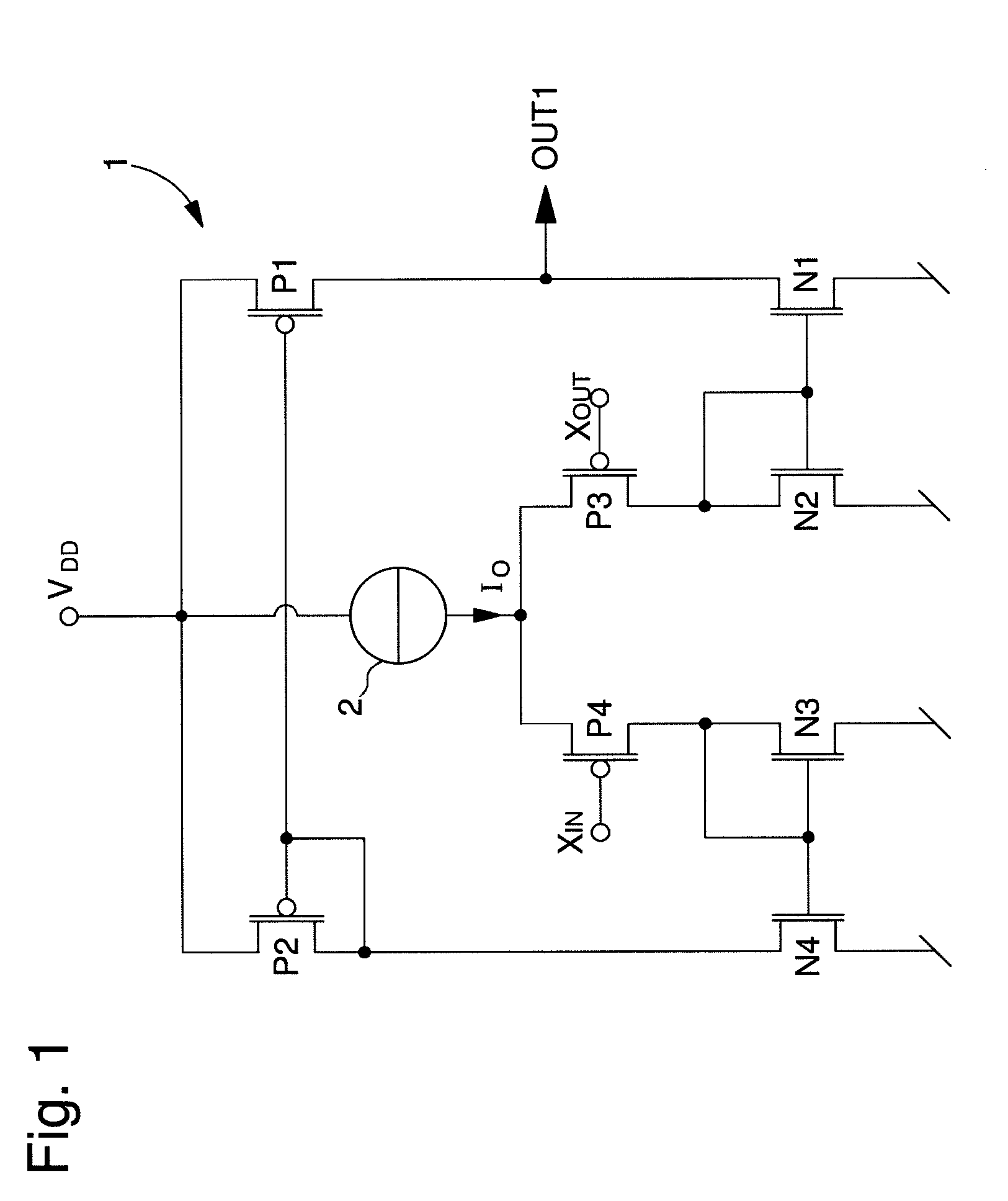
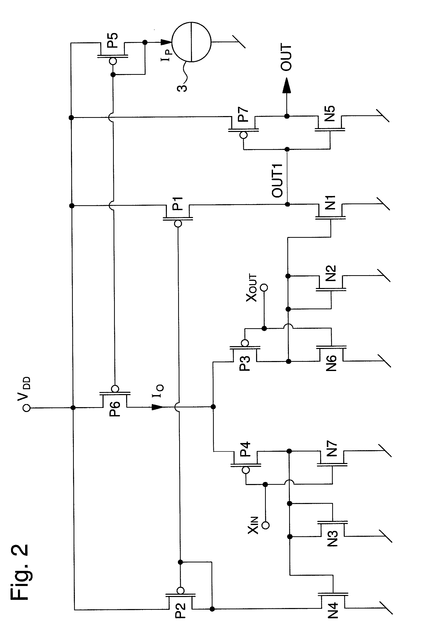
[0025]In the following description, those elements of the amplifier circuit that are well known to those skilled in this technical field will be related only in a simplified manner, particularly as regards how each transistor of the amplifier circuit is made. The amplifier circuit of the present invention is mainly used for supplying at least one clock or time base signal in electronic instruments, on the basis of oscillating signals in phase opposition from a quartz oscillator. The transistors described below are preferably MOS transistors, although one could also envisage making the amplifier circuit with bipolar transistors or a combination of MOS and bipolar transistors. In this regard, it is noted that each PMOS transistor described below defines a MOS transistor with a first type of conductivity, whereas each NMOS transistor defines a MOS transistor with a second type of conductivity, although the opposite could also be envisaged.
[0026]FIG. 2 shows a first embodiment of a low ...
PUM
 Abstract
Description
Claims
Application Information