Semiconductor device and method of fabricating the same

a technology of semiconductor devices and semiconductors, applied in semiconductor devices, semiconductor/solid-state device details, electrical apparatus, etc., can solve problems such as physical properties limitations, chip size reduction, and increase in the number of electric connection terminals, so as to improve physical and electrical properties

Inactive Publication Date: 2012-03-01
SAMSUNG ELECTRONICS CO LTD
View PDF7 Cites 1 Cited by
  • Summary
  • Abstract
  • Description
  • Claims
  • Application Information

AI Technical Summary

Benefits of technology

[0006]The inventive concept provides a semiconductor device having improved physical and electrical properties and a method of fabricating the semiconductor device.

Problems solved by technology

Accordingly, chip sizes are being reduced and the number of electric connection terminals are being increased, and thus, limitations caused by physical properties such as a size of the semiconductor device and electrical properties such as impedance of transferring lines have become severe.

Method used


Image

  • Semiconductor device and method of fabricating the same
  • Semiconductor device and method of fabricating the same
  • Semiconductor device and method of fabricating the same

Examples


Embodiment Construction

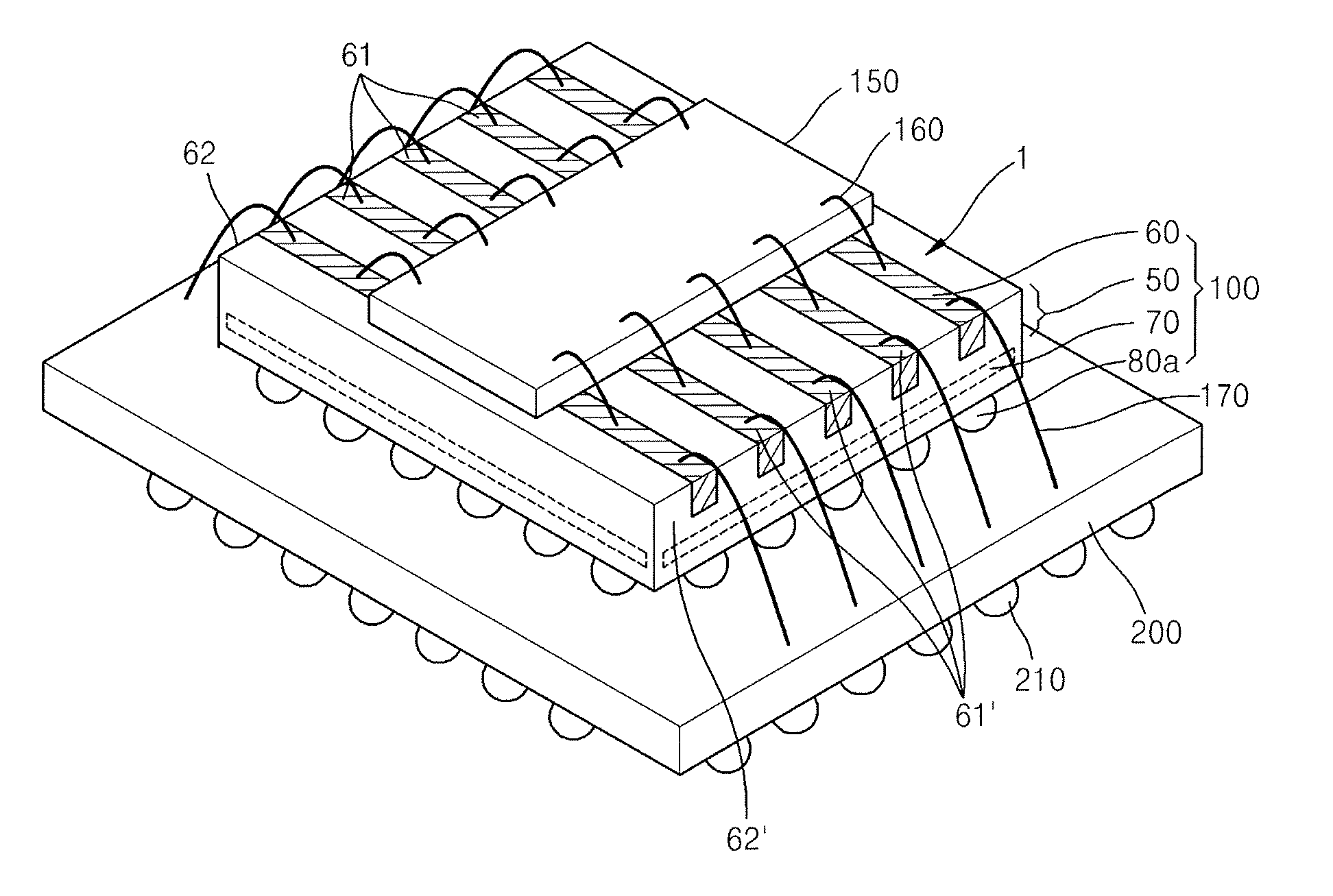
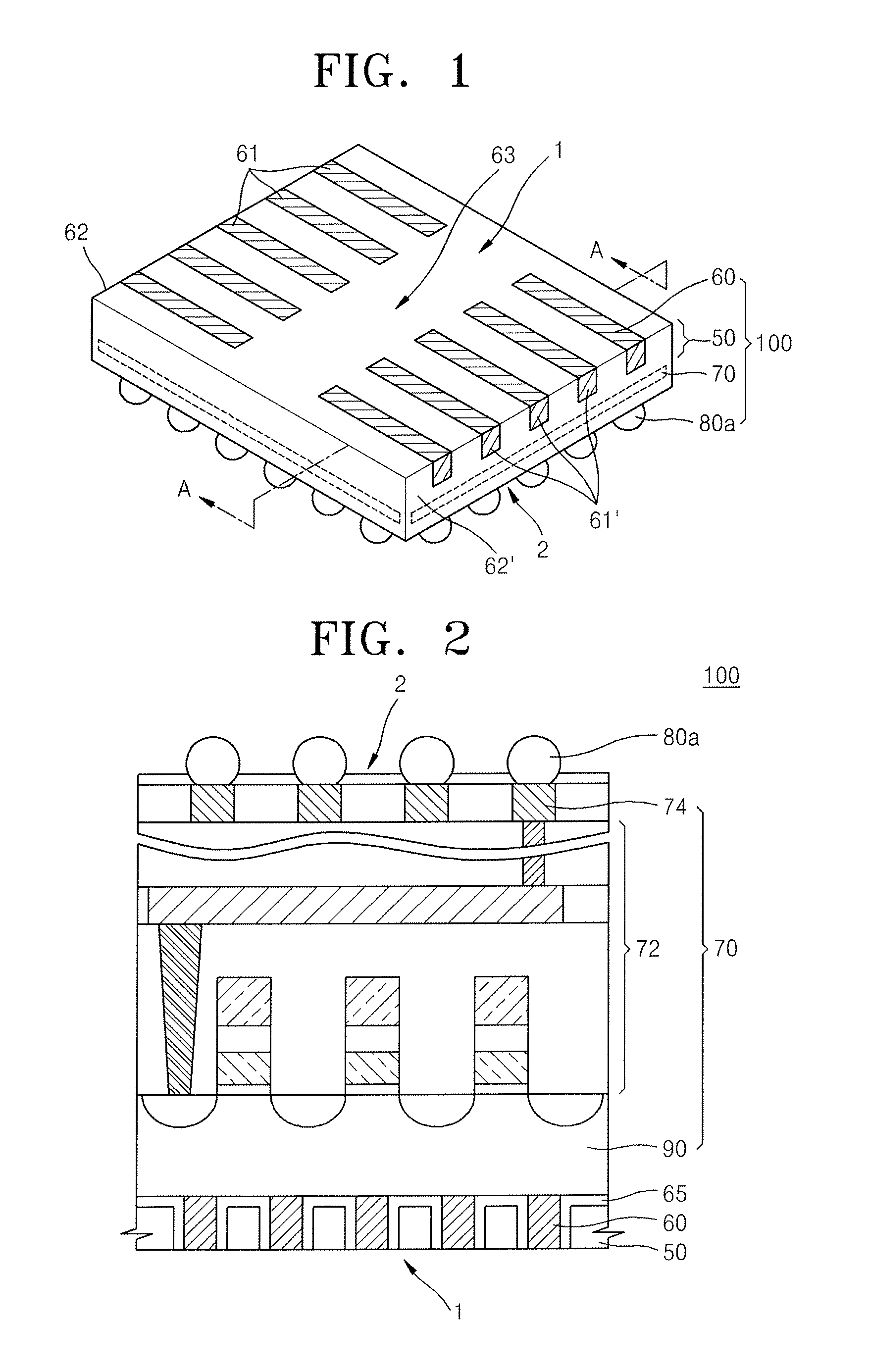
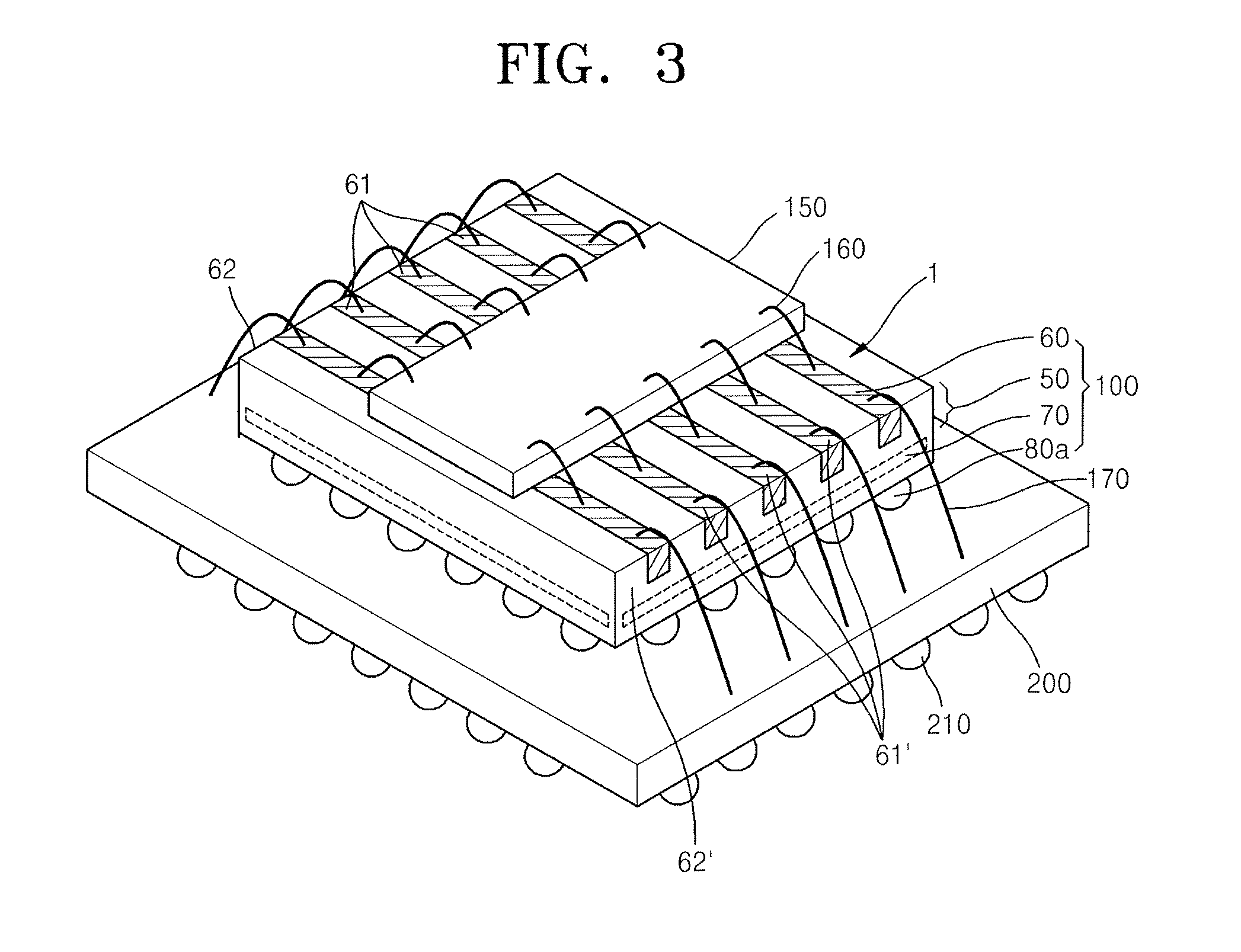
[0039]Reference will now be made in detail to exemplary embodiments of the present general inventive concept, examples of which are illustrated in the accompanying drawings, wherein like reference numerals refer to the like elements throughout. The exemplary embodiments are described below in order to explain the present general inventive concept while referring to the figures.

[0040]This present general inventive concept may, however, be embodied in many different forms and should not be construed as limited to the exemplary embodiments set forth herein; rather, these exemplary embodiments are provided so that this disclosure will be thorough and complete, and will fully convey the scope of the present general inventive concept to those skilled in the art. Although a few exemplary embodiments of the present general inventive concept have been shown and described, it would be appreciated by those skilled in the art that changes may be made in these exemplary embodiments without depar...


PUM


Abstract

A semiconductor device having improved physical and electrical properties includes a semiconductor chip comprising a first semiconductor substrate and a second semiconductor substrate on the first semiconductor substrate, conductive lines embedded in the first semiconductor substrate to be exposed on a surface of the first semiconductor substrate, a circuit structure formed on the second semiconductor substrate, and an external terminal formed on the circuit structure and electrically connected to the circuit structure, and an exposed surface of the first semiconductor substrate, where exposed surfaces of the conductive lines are located at the same plane.

Description

CROSS-REFERENCE TO RELATED APPLICATIONS[0001]This application claims priority under 35 U.S.C. §119(a) from Korean Patent Application No. 10-2010-0085511, filed on Sep. 1, 2010, in the Korean Intellectual Property Office, the disclosure of which is incorporated herein in its entirety by reference.BACKGROUND OF THE INVENTION[0002]1. Field of the Invention[0003]The inventive concept relates to a semiconductor device and a method of fabricating the semiconductor device, and more particularly, to a semiconductor device having improved physical and electrical properties and a method of fabricating the semiconductor device.[0004]2. Description of the Related Art[0005]Recently, demands for highly integrated and high performance semiconductor devices with small sizes have increased continuously. Accordingly, chip sizes are being reduced and the number of electric connection terminals are being increased, and thus, limitations caused by physical properties such as a size of the semiconductor ...

Claims


Application Information

Patent Timeline
Patent Type & Authority Applications(United States)
IPC IPC(8): H01L23/48
CPCH01L23/481H01L24/03H01L24/05H01L24/06H01L24/48H01L24/49H01L24/73H01L25/0652H01L25/0657H01L25/50H01L2224/0401H01L2224/04042H01L2224/05553H01L2224/0557H01L2224/056H01L2224/05624H01L2224/05647H01L2224/05657H01L2224/05666H01L2224/05684H01L2224/06181H01L2224/13027H01L2224/131H01L2224/16227H01L2224/32145H01L2224/48091H01L2224/48145H01L2224/48235H01L2224/4909H01L2224/4911H01L2224/49175H01L2224/73257H01L2224/73265H01L2224/97H01L2225/06506H01L2225/0651H01L2225/06517H01L2225/06541H01L2225/06568H01L2924/01013H01L2924/01029H01L2924/01032H01L2924/014H01L2924/09701H01L2924/14335H01L2924/1434H01L2924/1436H01L2924/1438H01L2924/1443H01L2924/15182H01L2924/15311H01L2924/01005H01L2924/01006H01L2924/01023H01L2924/01033H01L2924/01074H01L2924/01087H01L2924/3011H01L2224/16225H01L2924/00014H01L2224/85H01L2924/00H01L2224/023H01L2224/45099H01L2224/05599H01L2924/00012H01L2924/0001
Inventor YOO, JEONG-SIKLEE, SEOK-CHAN
Owner SAMSUNG ELECTRONICS CO LTD
Why Eureka
Try Eureka