Pixel structure and liquid crystal display panel having the same

a liquid crystal display and pixel structure technology, applied in the field of pixel structure and liquid crystal display panel, can solve problems such as mura defects, and achieve the effect of favorable transmittan

Active Publication Date: 2014-11-06
OPTRONIC SCI LLC
View PDF1 Cites 6 Cited by
  • Summary
  • Abstract
  • Description
  • Claims
  • Application Information

AI Technical Summary

Benefits of technology

[0006]The invention is directed to a pixel structure and an LCD panel having the same. Here, the pixel structure has favorable transmittance and is not prone to encounter the problem of the disclination lines.
[0010]As is discussed above, in the pixel structure and the LCD panel having the same, there is an opening at the edge of the pixel electrode adjacent to at least one of the scan line and the data line, and the portion of the metal layer extending to the edge of the pixel electrode is exposed by the opening. Hence, the liquid crystal material correspondingly arranged at the opening of the each pixel structures is not tilted toward the edge of the pixel structure. That is, in an embodiment of the invention, the liquid crystal material correspondingly arranged at the opening of each of the pixel structures is tilted toward the center of the pixel structure; thereby, the transmittance of the pixel structure is favorable, the issue of disclination lines is not apt to occur, and satisfactory display quality may be guaranteed.

Problems solved by technology

In a conventional PSA LCD panel, however, the edge of the pixel electrode is prone to encounter the problem of the disclination lines, which suffer the contrast and the transmittance of the LCD panel and further leads to the mura defect.

Method used


Image

  • Pixel structure and liquid crystal display panel having the same
  • Pixel structure and liquid crystal display panel having the same
  • Pixel structure and liquid crystal display panel having the same

Examples


first embodiment

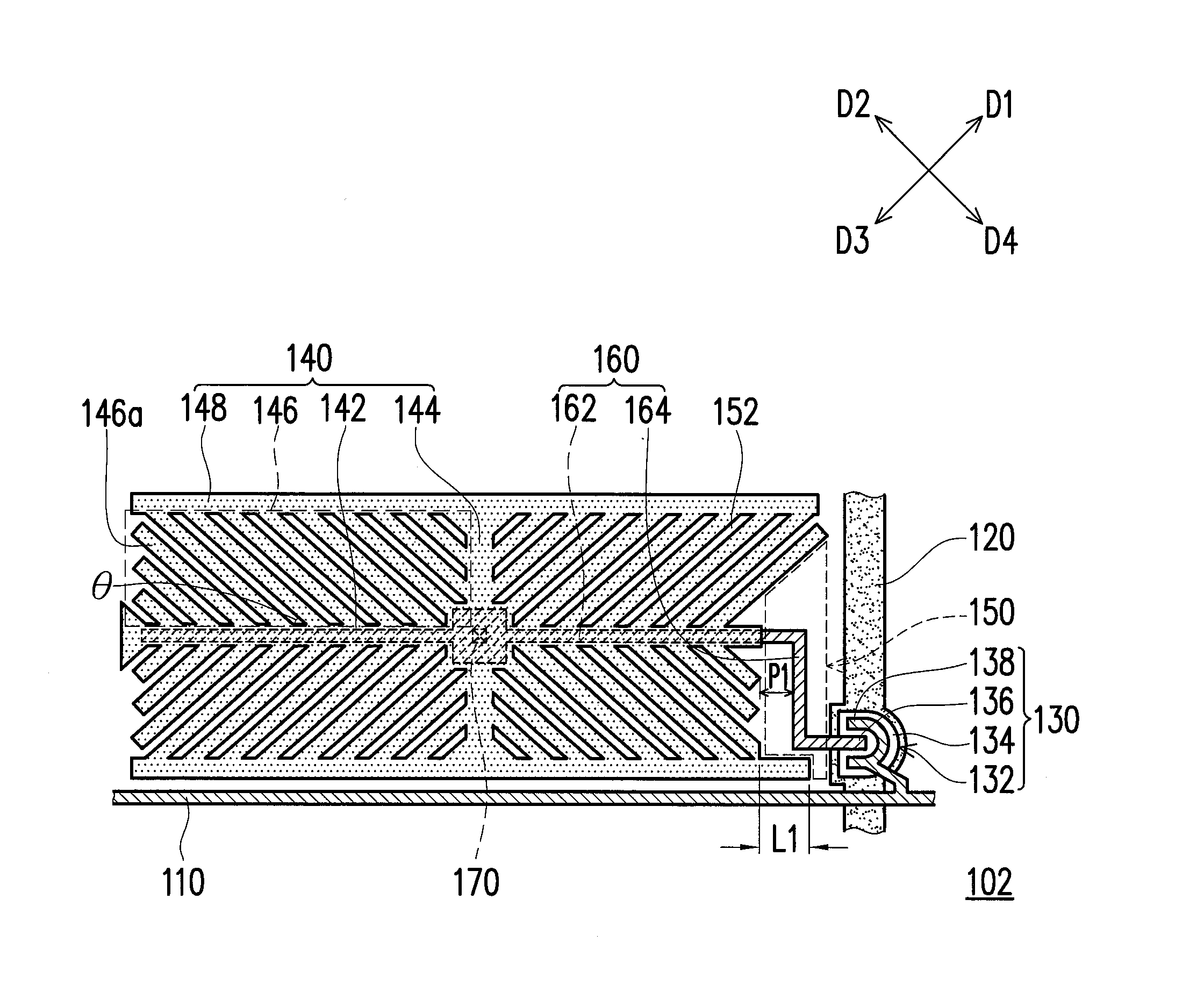
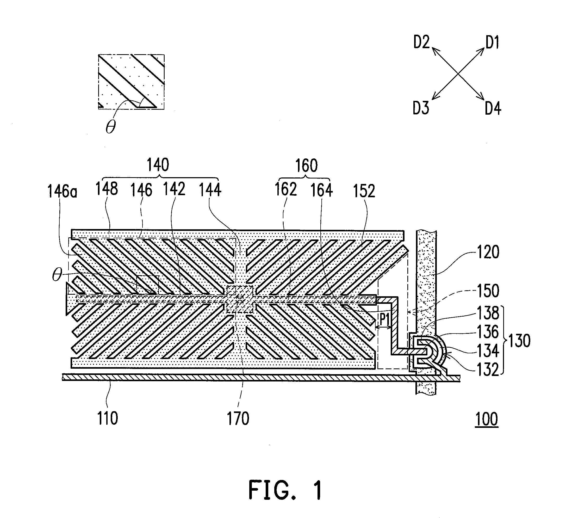
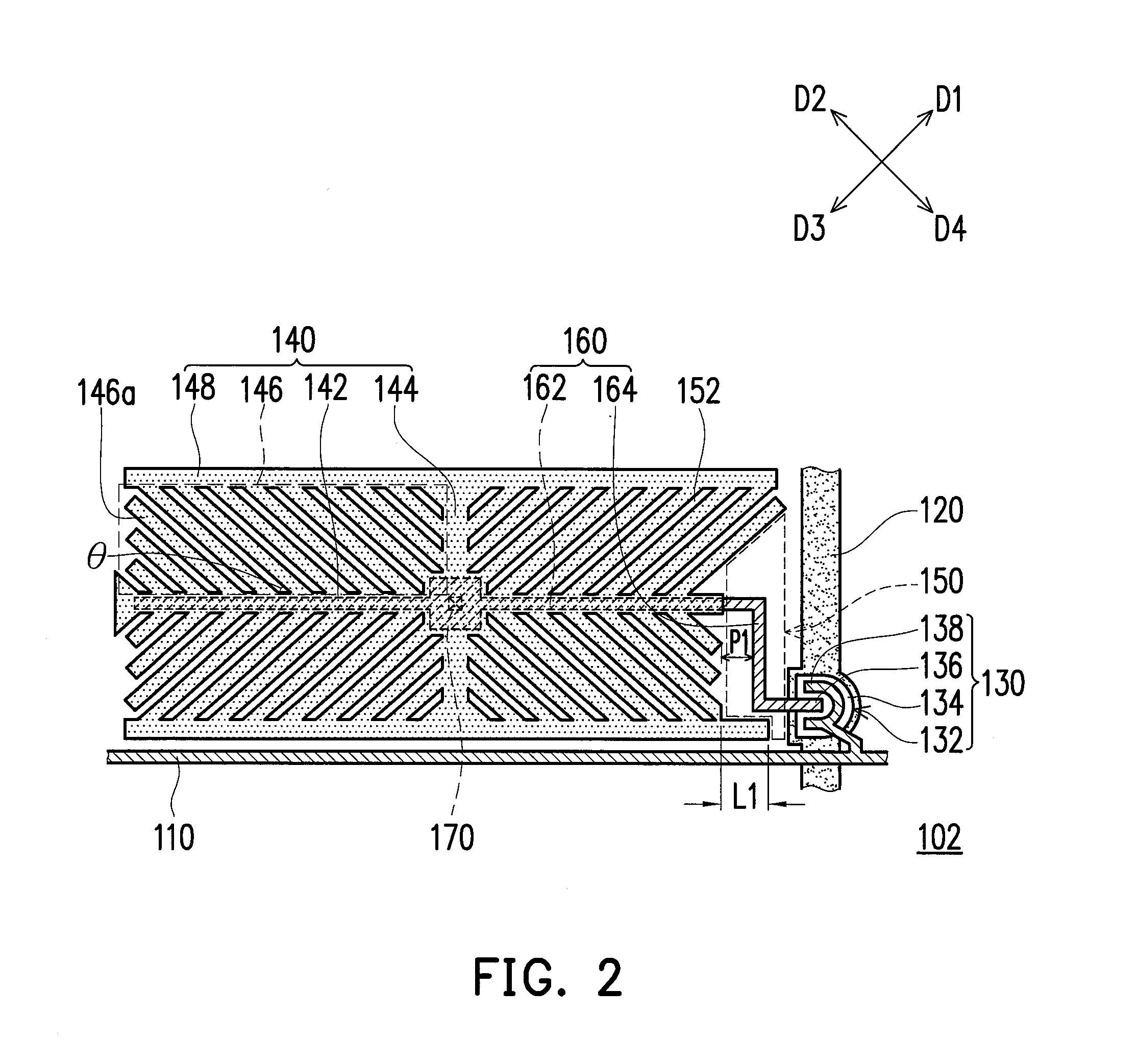
[0017]FIG. 1 to FIG. 5 are schematic top views illustrating a pixel structure according to the invention.

[0018]With reference to FIG. 1, the pixel structure 100 described herein includes a data line 110, a scan line 120, at least one active device 130, a pixel electrode 140, a metal line 160, and a contact window 170.

[0019]Extension directions of the data line 110 and the scan line 120 are not the same; preferably, the extension directions of the data line 110 and the scan line 120 are perpendicular to each other. In addition, the scan line 120 and the data line 110 are located at different film layers, and an insulation layer (not shown) is sandwiched therebetween. The scan line 120 and the data line 110 serve to transmit driving signals for driving the pixel structure 100. In general, the data line 110 and the scan line 120 are made metal, which should however not be construed as a limitation to the invention. According to another embodiment, the scan line 120 and the data line 11...

second embodiment

[0037]FIG. 6 is a schematic top view illustrating a pixel structure 200 according to the invention, and FIG. 7 is an enlarged view schematically illustrating an area R depicted in FIG. 6. With reference to FIG. 6 and FIG. 7, the embodiment shown herein is similar to the embodiment shown in FIG. 1, so that identical components in these figures will be denoted by the same numerals and will not be reiterated herein. The difference between the embodiment shown in FIG. 6 and the embodiment shown in FIG. 1 rests in that the opening 250 at the edge of the pixel electrode 140 adjacent to the scan line 120 is a close-ended opening, and the first portion 162 and the second portion 164 of the metal line 160 are parallel to each other. Here, the second portion 164 (e.g., the metal line segment 164′) is partially exposed by the opening 250. However, the invention is not limited thereto, and in another embodiment, the opening 250 may be adjacent to at least one of the data line 110 and the scan l...


PUM

PropertyMeasurementUnit
distanceaaaaaaaaaa
distanceaaaaaaaaaa
distanceaaaaaaaaaa

Abstract

A pixel structure and a liquid crystal display (LCD) panel having the same are provided. The pixel structure includes a data line, a scan line, at least one active device, a pixel electrode, and a metal line. The active device is electrically connected to the data line and the scan line. The pixel electrode is electrically connected to the active device and has an opening at the edge of the pixel electrode adjacent to at least one of the data line and the scan line. The metal line is located below the pixel electrode. Besides, a portion of the metal line extending to the edge of the pixel electrode is exposed by the opening. The shortest distance between an edge of the opening of the pixel electrode and the metal line is greater than or substantially equal to 3 μm.

Description

CROSS-REFERENCE TO RELATED APPLICATION[0001]This application claims the priority benefit of Taiwan application serial no. 102116109, filed on May 6, 2013. The entirety of the above-mentioned patent application is hereby incorporated by reference herein and made a part of this specification.BACKGROUND OF THE INVENTION[0002]1. Field of the Invention[0003]The invention relates to a pixel structure and a liquid crystal display (LCD) panel having the same; more particularly, the invention relates to a pixel structure to which a polymer stabilized alignment (PSA) technique is applied and an LCD panel having the pixel structure.[0004]2. Description of Related Art[0005]As the LCD technology continuously progresses in a direction of providing a large display screen, the market has been gravitating toward the LCDs characterized by high contrast ratio, rapid response, wide viewing angle, and so forth. Therefore, the wide viewing angle techniques of the LCD panels are continuously developed in ...

Claims


Application Information

Patent Timeline
Patent Type & Authority Applications(United States)
IPC IPC(8): G02F1/1362H01L33/36
CPCG02F1/136286H01L33/36G02F1/133707G02F1/134336G02F1/13775
Inventor CHUNG, JEN-YANGTIEN, KUN-CHENGWANG, CHENGWEI, WEI-CHUNWU, MING-HUEIGONG, SHIN-MEILIAO, CHIEN-HUANG
Owner OPTRONIC SCI LLC
Why Eureka
Try Eureka