
Snap-action switch
- Summary
- Abstract
- Description
- Claims
- Application Information
AI Technical Summary
Benefits of technology
Problems solved by technology
Method used
Image

Examples
Embodiment Construction
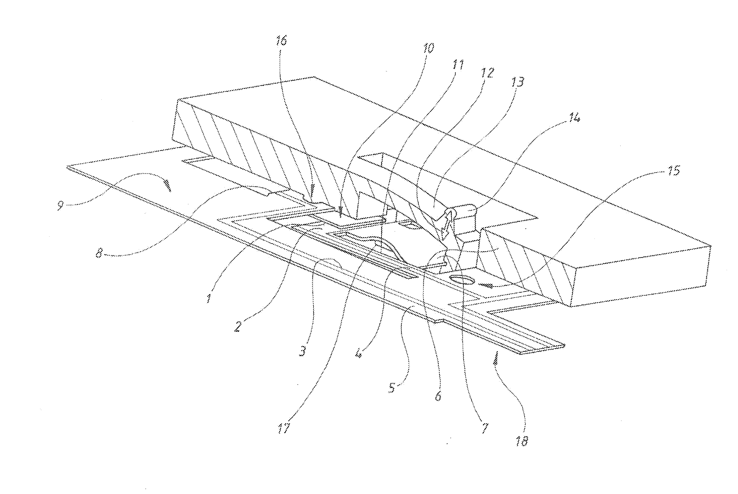
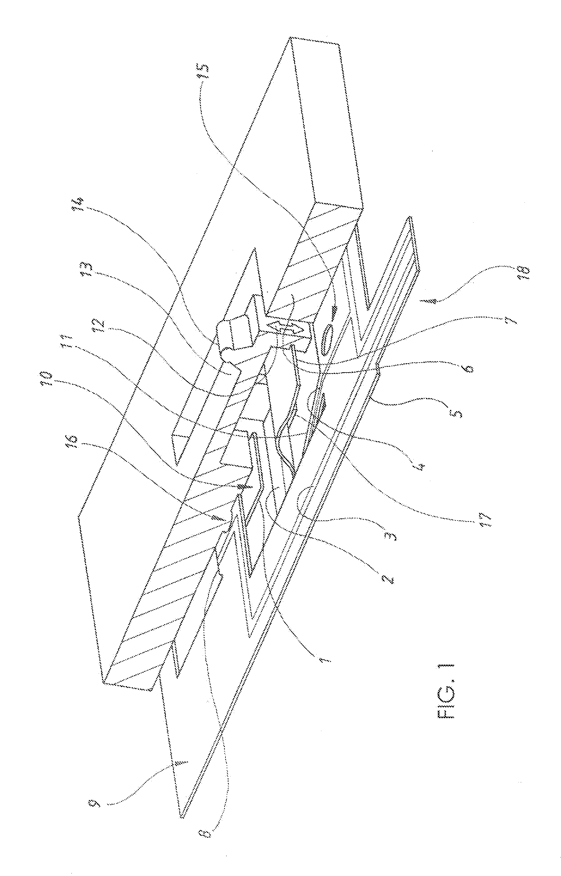
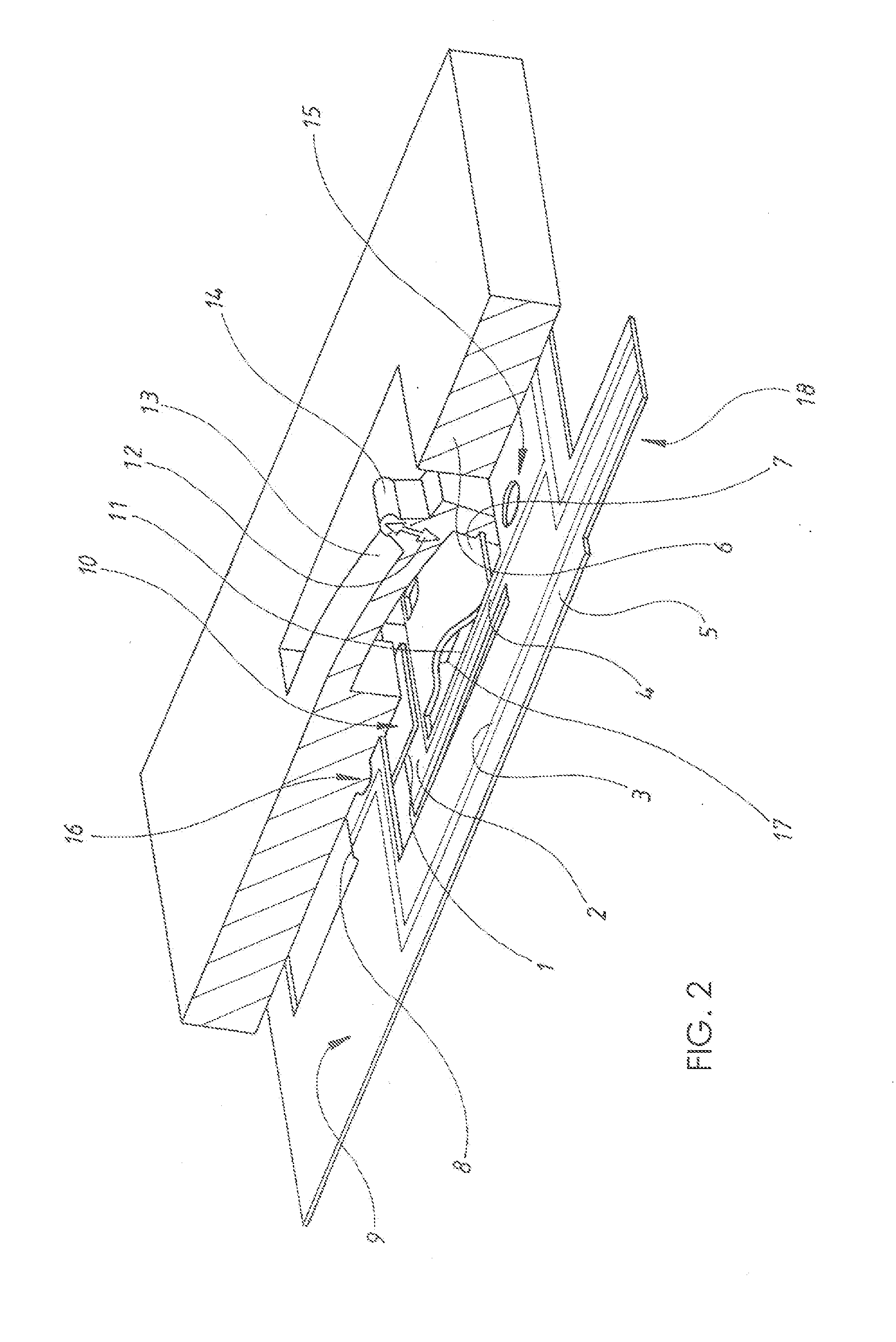
[0037]FIG. 1 shows a perspective partial view of a snap-action switch according to the invention, with two switching contacts 1, 2, a flexible circuit carrier 5 having conductor tracks 3, 4 and a multi-function component 6 receiving the flexible circuit carrier 5. For better understanding of the constructional switch design, FIG. 1 shows only one half of the multi-function component 6 divided into two halves by a mirror-symmetrical section. The underside of the multi-function component is shown in FIG. 7 and the underside of the assembled switch is shown in FIG. 8. The switching contacts 1, 2 are print-ons applied to the conductor tracks 3, 4 of the flexible circuit carrier 5. A region of the flexible circuit carrier 5 between the switching contacts 1, 2 is configured as a bending tab 7. Since the conductor tracks 3, 4 are both formed on the same side of the flexible circuit carrier 5, the carrier comprises a turn-over fold 8 formed between its switching contacts 1, 2. In addition t...
PUM
| Property | Measurement | Unit |
|---|---|---|
| Flexibility | aaaaa | aaaaa |
Abstract
Description
Claims
Application Information