
Snap-action switch

a technology of sliding contact switch and action switch, which is applied in the direction of emergency connections, contacts, emergency contacts, etc., can solve the problems of affecting the service life of the switch with sliding contact, affecting the service life of the switch, and deteriorating electric characteristic values, etc., to achieve the effect of reducing weight, simple operation, and reducing weigh

Active Publication Date: 2017-04-18
KOEPSELL MARTIN
View PDF12 Cites 0 Cited by
  • Summary
  • Abstract
  • Description
  • Claims
  • Application Information

AI Technical Summary

Benefits of technology

[0014]Thus in the simplest case, the snap-action switch according to the invention is composed of only two components, wherein one of the components is the multifunction component and the other is the flexible circuit carrier. In order to achieve its function as per the invention the bending tab is exposed to a bending or buckling stress by tensioning the flexible circuit carrier in the multifunction component, thereby creating an energy potential transmitter for the snap action function in order to effect a reversible geometry change. Together with the bending tab the flexible circuit carrier plays an important and direct part in the configuration of the switching mechanics. With a construction composed of very few, in particular two components the snap-action switch according to the invention is constructed in a very simple, weight-reduced and reliably working manner. In addition the snap-action switch according to the invention, due to its small number of components, is extraordinarily insensitive to variations in size due to the manufacturing process and permits maximum weight reduction for a minimum of material used.
[0015]According to a first further development of the invention the switching contacts are print-ons applied to the conductor tracks of the flexible circuit carrier. With the print-ons the configuration of the switching contacts is preferably part of the manufacture of the circuit carrier and is no longer part of the assembly process of the snap-action switch according to the invention. The snap-action switch according to the invention therefore does not comprise any connection contacting between its switching contacts and its flexible circuit carrier resulting in a complete lack of error potential. The manufacture of the conductor tracks is preferably effected by coating the entire area of the carrier material by means of an electric conductor such as copper and then removing the copper by etching the spaces between the conductor tracks. Alternatively the conductor tracks may be manufactured by applying print-ons to the flexible circuit carrier. Manufacture of the switching contacts is also partially effected by print-ons applied to the conductor tracks of the flexible circuit carrier, wherein one of the switching contacts is a silver print-on and the respectively other switching contact is a carbon print-on. With the silver and copper material pairing in the contact region of the switching contacts the snap-action switch according to the invention comprises an almost constant bounce time as well as an almost constant electric resistance over its entire period of use. By using switching contacts produced by way of printing and conductor tracks also produced by way of printing there is, advantageously, no longer any need for electroplating individual components or regions of the snap-action switch according to the invention. In addition the flexible circuit carrier comprises a coating with cut-outs for the switching contacts, and this coating protects the conductor tracks thereof against environmental influences.
[0017]According to a next further development of the invention the conductor tracks are formed on at least one side of the flexible circuit carrier, wherein the flexible circuit carrier comprises at least one turn-over fold formed between its switching contacts. The turn-over fold is used to spatially bring the switching contacts together for the purpose of direct contacting. A particularly flat shape for the snap-action switch according to the invention is achieved if the turn-over fold is designed with a sharp edge and areally adjacent circuit carrier areas. On the other hand, it is well within the scope of the invention to configure the turn-over fold as a soft bending fold with a loop-shaped circuit carrier area. The turn-over fold advantageously permits the use of easy-to-produce flexible circuit carriers with only a single conductor track plane for, at the same time, a constructionally simple design of the inventive snap-action switch.
[0019]With the snap-action switch according to the invention a bi-stable switching characteristic is achieved in that a knocking tab is formed with at least one of the overlapping circuit carrier portions of the flexible circuit carrier, which is held under tension in the multifunction component via the bending tab. The knocking tab ensures that ideally no relative movements occur between the switching contacts during opening and closing of a circuit, thereby preventing any possible wear due to abrasion in the contact region of the switching contacts. Due to the switching contacts areally knocking against each other the snap-action switch according to the invention advantageously comprises a short bounce time and generates very little noise. Any switching noises which might occur, can be advantageously dampened by selecting sound-absorbing plastics for the carrier material of the flexible circuit carrier. The short bounce times mean that the snap-action switch according to the invention is suitable also for switching signal currents which is a very challenging activity. The snap-action function is achieved in that the multifunction component makes the bending tab of the snap-action switch according to the invention bend or buckle, and the restoring force of this creates a triangle of forces between the multifunction component, the knocking tab and the bending tab, in which an elastic deformation of the flexible circuit carrier leads to an abrupt direction reversal of the resultant load from the triangle of forces. With the bi-stable switching characteristic such a direction reversal of the resultant load causes the knocking tab to immediately change from one switching position to the other, respectively.

Problems solved by technology

While in the dead path of the actuating structure both the opening and the closing circuits are open so that the actuating structure may have a negative influence upon the switchover time.
The service life of switches with sliding contacts is substantially limited by abrasions occurring on the sliding contacts.
In the course of this service life the electric characteristic values deteriorate as a result of this wear from abrasion, in particular the resistance of the switch deteriorates depending on the number of actuating and temperature cycles of switching operations carried out.
At low temperatures, when the viscosity of the lubricant is reduced, the electric characteristic values deteriorate, in particular electric resistances rise and the switchover times of switches lengthen.
The use of precious metals however makes manufacture of the switches very expensive.
However continuous electroplating is a highly specialized and capital-intensive manufacturing process which requires setting up an external supply chain.
Such supply chains are however disadvantageous when aiming at vertical manufacturing depth, small batch sizes, low stocks and flexibility in changing process variables.
The junctions however remain a cause for functional failure.
In many areas however, the demand is now for low-noise or nearly noiseless switches because noises arising from switch actuation are perceived as increasingly annoying.
With this design the number of components, albeit, is reduced, but it comprises soldering points which are susceptible to failure.

Method used


Image

  • Snap-action switch
  • Snap-action switch
  • Snap-action switch

Examples


Embodiment Construction

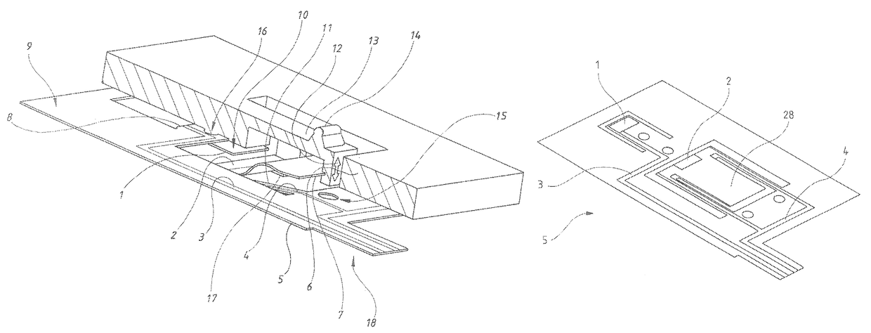
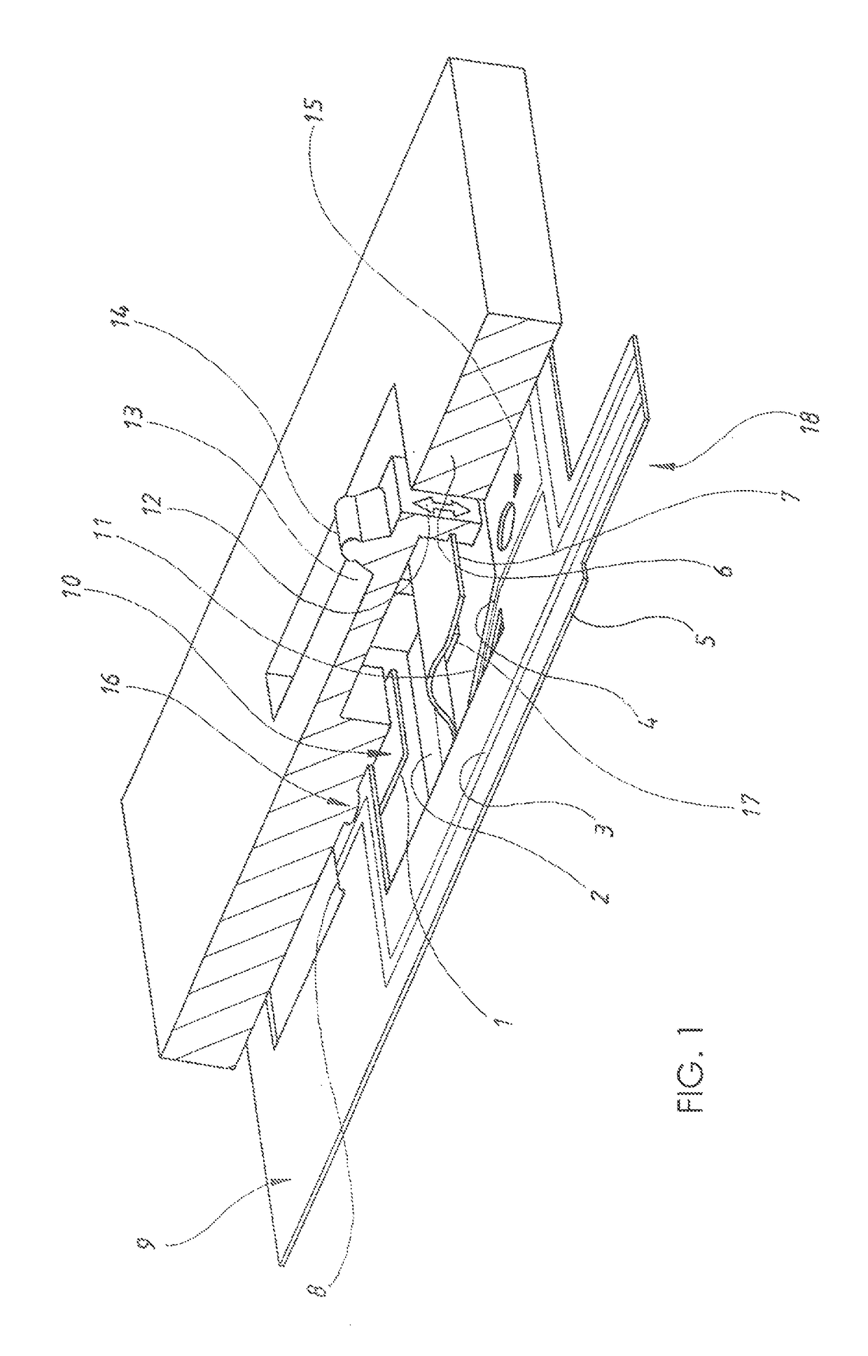
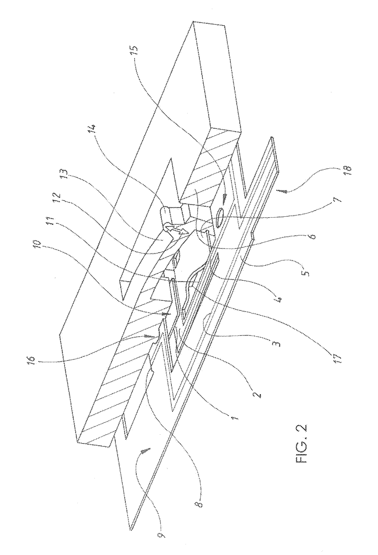
[0037]FIG. 1 shows a perspective partial view of a snap-action switch according to the invention, with two switching contacts 1, 2, a flexible circuit carrier 5 having conductor tracks 3, 4 and a multi-function component 6 receiving the flexible circuit carrier 5. For better understanding of the constructional switch design, FIG. 1 shows only one half of the multi-function component 6 divided into two halves by a mirror-symmetrical section. The underside of the multi-function component is shown in FIG. 7 and the underside of the assembled switch is shown in FIG. 8. The switching contacts 1, 2 are print-ons applied to the conductor tracks 3, 4 of the flexible circuit carrier 5. A region of the flexible circuit carrier 5 between the switching contacts 1, 2 is configured as a bending tab 7. Since the conductor tracks 3, 4 are both formed on the same side of the flexible circuit carrier 5, the carrier comprises a turn-over fold 8 formed between its switching contacts 1, 2. In addition t...


PUM

PropertyMeasurementUnit
flexibleaaaaaaaaaa
switchover timeaaaaaaaaaa
snap-action timeaaaaaaaaaa

Abstract

A snap-action switch has at least two switching contacts, at least one flexible circuit carrier carrying conductor tracks and at least one multifunction component receiving the flexible circuit carrier. The switching contacts and the conductor tracks are connected with each other via a non-detachable connection. The region of the flexible circuit carrier between the switching contacts is configured as a bending tab.

Description

CROSS REFERENCE TO RELATED APPLICATIONS[0001]This non-provisional patent application claims priority under 35 U.S.C. §119(a) from Patent Application No. 102013018448.7 filed in Germany on Nov. 5, 2013, the entire contents of which are hereby incorporated by reference.FIELD OF THE INVENTION[0002]This invention relates to a snap-action switch with at least two switching contacts, at least one flexible circuit carrier carrying conductor tracks and at least one multi-function component receiving the flexible circuit carrier. In addition this invention relates to a method of manufacturing a snap-action switch from at least two switching contacts and at least one flexible circuit carrier carrying conductor tracks.BACKGROUND OF THE INVENTION[0003]Generic snap-action switches, also known as “jump” switches, are switches where the switching positions are formed by reversible geometry changes of their movable switching contacts. When switching these snap-action switches the switching position...

Claims


Application Information

Patent Timeline
Patent Type & Authority Patents(United States)
IPC IPC(8): H01H9/00H01H1/58H01H5/04
CPCH01H5/04H01H1/5805H01H2001/5816H01H2207/04Y10T29/49105
Inventor KOEPSELL, MARTIN
Owner KOEPSELL MARTIN
Learn More